The production level CMP tool will be approximately 6 feet tall and 8 feet in diameter. It has a large round table which can rotate. Some variants of the tool make linear or a combination of linear and sidewise movement. On top of the table, a soft material called pad will be present. The wafer will be help upside down and pressed onto the pad. The tool has facilities to control the pressure at various points of the wafer. A slurry, which is a combination of chemicals and abrasive particles, will be made to flow between the wafer and the pad. The wafer and the table will move and the relative movement will cause removal of material. (Figure 4.10). The removal rate depends on the pressure, the speed of rotation, the concentration of chemicals in the slurry and the particle nature and size.
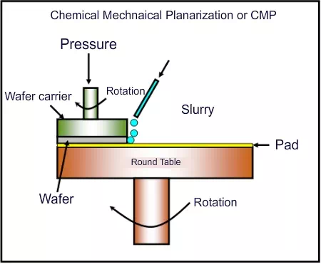
Figure 4.10. Schematic of Chemical Mechanical Polisher
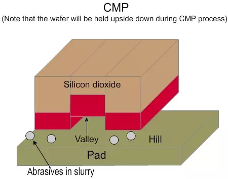
Figure 4.11. Schematic of wafer at the beginning of CMP
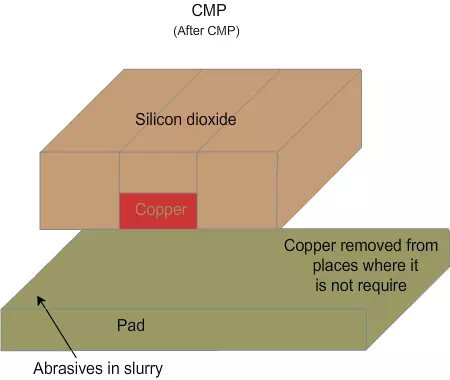
Figure 4.12. Schematic of wafer at the end of ideal CMP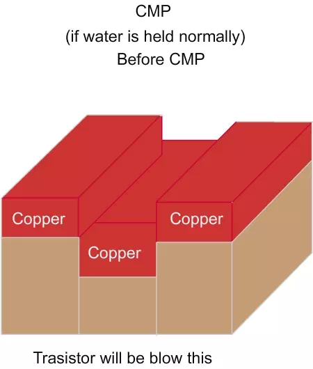
Figure 4.13. Schematic of wafer in the beginning of CMP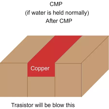
Figure 4.14. Schematic of wafer at the end of CMP
What is the role of chemical and what is the role of abrasive? The chemicals are necessary for obtaining selectivity. i.e. if one material has to be removed and another material should not be removed, the slurry should contain a suitable chemical. For example, in Fig 4.7, copper has to be removed and silicon dioxide should not be removed. For this, a chemical which dissolves copper and not silicon dioxide should be chosen. When all the copper over silicon dioxide is polished, the silicon dioxide will not be removed. The particles or abrasives are needed to obtain a planar surface. The higher levels (peaks or hills) will be removed faster while the material at the lower level (valley ) will be removed slowly. Thus the wafer will be planarized.
For example, to remove excess copper, a slurry containing nano size silicon dioxide particles (abrasives) and chemicals such as oxidizers, complexing agents and corrosion inhibitors. The pad is made of a polymer material such as poly urethane. For removal materials like silicon dioxide, a hard pad is used, while a soft pad is used for removing materials like copper. Here, the terms soft and hard are used in a relative sense. A soft pad may be similar to ‘puff’ used for applying powder to the face, while the hard pad may have a texture and feel similar to that of a leather bag. There are two goals in CMP. One is to remove excess material and the second is to planarized the surface. When a material is deposited on wafer, it may not be deposited uniformly. CMP can be used to planarized such surfaces also.
Dishing and erosion:
Two of the major issues that arise during CMP are dishing and erosion. Consider the set large copper wire shown in figure 4.15. Before planarization, the deposited copper film will look as shown in fig 4.15a. After planarization, ideally, the surface must be flat as shown in fig 4.15b. However, the pad is not a perfectly rigid and straight body and it can in fact bend slightly. Because of that, the copper will be removed as shown in fig 4.15c. This unwanted removal of copper, leading to non planar surface and high resistance wire is called dishing. This occurs especially on wide lines.
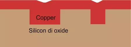
Figure 4.15 a. Schematic of wafer (a) before CMP

Figure 4.15 b. Schematic of wafer after CMP (ideal case)
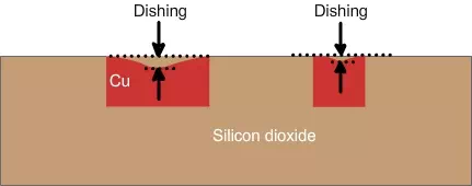
Figure 4.15 b. Schematic of wafer after CMP (real case). Note the dishing in real CMP.
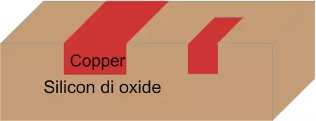
Figure 4.16 a. Three dimensional view of the lines in figure 6.15 (b).
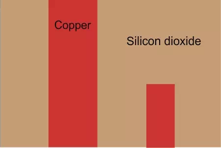
Figure 4.16 b. Top view of the same structure.
The same wire is shown in the top view in fig 4.16, after ideal planarization. The percentage of area occupied by copper in the top view is called aerial density. To calculate the aerial density , a square of perhaps 10 micron size is usually considered. When the density is higher, dishing and the related issue, erosion, become more likely. Two samples are shown in Fig. 4.17 a and b.
Copper aerial density is 20%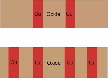
Copper aerial density is 40%
Fig. 4.17 a and b. Illustrations of locations with different aerial densities. Top view is shown
The loss of silicon dioxide by copper CMP process is called erosion and is illustrated in figure 4.18. When there are many copper lines nearby and in general when the copper aerial density is high, the oxide between the copper is also likely to be removed. This is because the oxide in this area will experience a higher pressure during the CMP process.
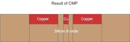
Figure 4.18 a. Result of CMP (ideal case).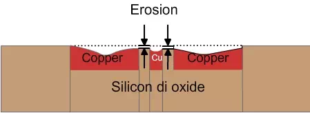
Fig 4.18 b. Result of real CMP (with Erosion ) Note the erosion i.e. the undesirable loss of oxide
Slotting and dummy fill: In order to provide fairly uniform aerial density, two features called “slotting” and “dummy fill” are used. Consider a wide copper line, shown in the top view (fig.4.19a). The aerial density can be reduced by decreasing the line width, but this will increase the electrical resistance. Instead, the line is made even wider, but islands of oxide are introduced in the line (fig 4.19b). This is also called “introduction of slots” or “slotting”. This will prevent excessive dishing during CMP.
Similarly, if an area does not contain copper at all, because there are no connections needed in that location, it will have only oxide (fig. 4.20b)
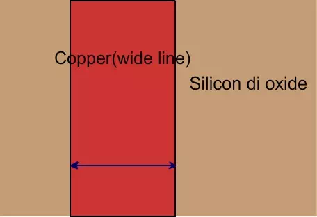
Figure 4.19 a. Top view of a wide line before slotting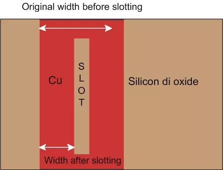
Figure 4.20. b. Top view of the same line after slotting. Note that the new line is wider than the original line in some places, but in most places, the width is less after introduction of slot
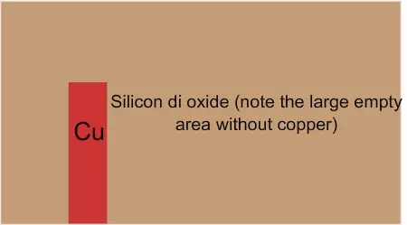
Figure 4.20 a. Top view of an area before dummy fill.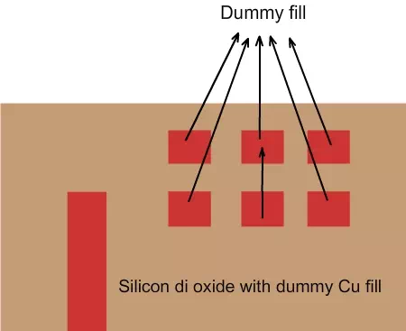
Figure 4.20 b. Top view of an area after dummy fill.
In these cases, a few islands of copper are added in the layout. Note that these copper lines will not connect to any other line and do not serve any purpose in the final chip. They are introduced only to ensure that the CMP process will planarized the chip properly. This is similar to adding protective diodes connected to aluminum islands to avoid ESD during dry etch.
If the aerial density varies a lot in the chip, the CMP process will not be able to planarized the surface effectively. Slotting will reduce the density from very high value to an acceptable value. Dummy fill will increase the density from very low value to an acceptable value. Together, these two tricks are used to convert the layout to a process friendly form. Copper interconnects have become part of the IC manufacturing only after copper CMP was introduced. Before that, although the scientists attempted using dry or wet etch to create copper lines, they were not successful in a commercial scale. In the early 1990s IBM engineers created chips with copper lines. Since CMP enabled the introduction of copper wires, it is called enabling technology. The fact that many small devices like cell phones and laptops can run on a battery for a long time is due to the fact that copper wires are used in the ICs.
CMP also plays a key role in electrically isolating transistors. A technique called shallow trench isolation (STI) is used to keep the transistors electrically isolated. While silica abrasives are used for Cu CMP slurries, silica or ceria abrasives are used for STI CMP slurries. The details of STI and the role of CMP process in STI is described in the front end of line (FEOL) section. In the next section we will see the three techniques used to modify the material viz. 1. Ion implantation, 2. Diffusion and 3. Oxidation.