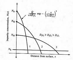
Dopant redistribution: The doped silicon is oxidized in some places, as part of the process sequence. The dopants which are present on the surface would be incorporated in the oxide, as expected. However, because of the formation of oxide, the dopants may re-distribute. If we consider two immiscible liquids, with a common solute, then the solute will preferentially move to one phase. This principle is used in liquid-liquid extraction in chemical industries. Here, we have two solid phases, viz. silicon dioxide and silicon. The solubility of the dopant in these two phases is different and hence redistribution occurs. The diffusivity of the dopant in these phases will also be different. Thus, the concentration profile, after oxidation, can vary in different ways, as shown below.
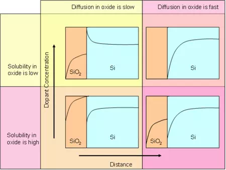
Figure 6.7. Qualitative plots showing dopant redistribution under various solubility and diffusivity conditions
Thus, the final profile of dopant in the transistor will change depending on the processes such as oxidation that occur after doping.
Lateral diffusion:
Although the doping is desired only in certain locations, the diffusion occurs in all directions. For example, the schematic below shows the desired doping in the ideal case and the doping that would occur in the real case.
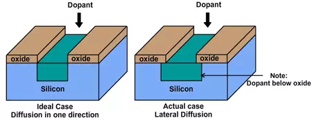
Figure 6.8. Schematic illustrating the lateral diffusion effect
When the transistors are separated by relatively large distance (a micron or more), the lateral diffusion was not a significant issue. When the distance between the transistors are small, and when the distance between a source and the drain in the same transistor is small, then lateral diffusion causes short-circuiting. Hence methods that eliminate this problem must be used. Ion implantation is a method which can mitigate this issue to some extent and we will learn about that in the next section.
Gettering: Gettering is the process of trapping unwanted impurities in a place away from the active region. Active region is the region where transistors are created, i.e. it is the region near the front surface. If unwanted impurities are present in Si, then it is desirable to move them to the back of the wafer rather than leave them on the front, active, side. This is achieved by one of the following techniques. The impurities tend to move towards crystal defects. All these techniques involve creating crystal defects of one form or another. In one technique, the back side of the wafer is doped with high concentrations of Phosphorous. In another, argon implantation is performed on the back side, leading to defects. In the third technique, silicon nitride film is deposited on the back side and this leads to stress, which leads to defects. Adding slight amount of oxygen during the Si crystal growth itself is another technique that can help trap the defects. Even if the defects are near the active area, if they are trapped and made immobile, then the life of the chip will be longer.
Sheet resistance: When the wafer is doped, the conductivity of the material increases. The level of doping can be estimated by measuring the conductivity. In IC industry, a quantity called sheet resistance is often measured and reported. Here we will learn about the concept of sheet resistance.
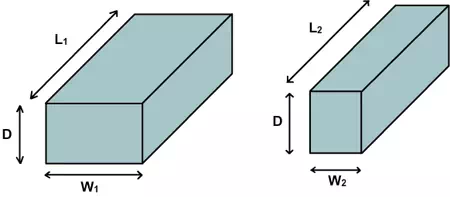
Figure 6.9. Schematic of two lines with the same depth, but different lengths and widths.
Consider two metal lines of same depth (D), but with different width and lengths. For example, in metal 2 layer, the depth is given by the deposition process, but the length and widths of lines are given by the lithography process (mask). Hence all lines in metal 2 will have same depth but different length and widths.
A top view of the same lines will appear as follows.
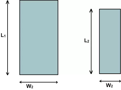
Figure 6.10. Top view of the two lines shown in fig. 6.9
The resistance of the first and second lines are given respectively by ![]() and
and ![]() ,
,
where r is the resistivity of the material. Since the depth is the same for both lines, the resistance is proportional to the ratio of length to width. The ratio of resistivity to depth is called “sheet resistance”. The ratio of length to width is also called “number of squares”. When the ratio of length to width is one, then the top view will appear as a square. For a given layer, the resistance of each square is the same, regardless of the size of the square. In the top view, if we try to fit a large square in the rectangle, the first line can accommodate two large squares. The second line can accommodate three squares
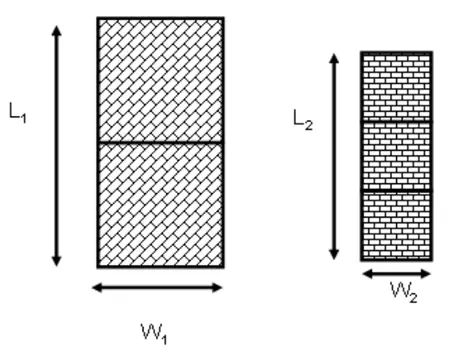
Figure 6.10. Top view of the two lines shown in fig. 6.9, with number of squares illustrated
For a given layer (i.e. when the material and the depth are fixed), the sheet resistance is a constant and is expressed as ‘ohm/square’ or sometimes written as “ohm/□’. Then the resistance of a line is calculated as the product of sheet resistance and the ‘number of squares’ in the line (from the top view).