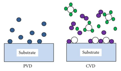
We saw that during deposition, it is not possible to deposit a material only in the places that we need. The material will get deposited in excess and throughout the wafer. This excess material and the material in unwanted places must be removed. The removal has to be done carefully, as otherwise material may also be removed from places where it is actually needed. Thus, the removal is relatively slow. A fast removal of material may be called dissolution, while the slow removal that is used in IC manufacturing is called etching. Removal of excess material is a stage in IC manufacturing. Typically, there will be a chemical reaction. Three types of removal techniques are employed in this. (1) Removal by using liquids, called wet etching (2) removal by using gases, called “dry etching” and (3) removal by using liquids, abrasives and pressure, called “chemical mechanical planarization”.
Wet etching.
In this method, a solution which can etch the material will be kept in a tank and the wafer will be dipped in the tank for a given time, at a given temperature. The excess material will dissolve or be etched from the wafer. There will be facilities to maintain the temperature and mix the solution well, in order to maintain uniformity. 10 or 20 or 25 wafers may be etched at the same time. After etching, the wafers will be taken out and rinsed in DI water and dried by spinning. If it is dried without spinning, some water may remain on the wafer leaving certain marks, called ‘water marks’. It is difficult to deposit or etch material in those locations. Hence spin drying is employed. Even with spin drying, watermarks may form sometime, and in order to avoid it, isopropyl alcohol (IPA) is used for final rinse and spin drying.
For almost all materials, there is some solvent which can etch it. Silicon dioxide is used in IC manufacturing at various stages. Silicon dioxide is just pure glass. It doesn’t dissolve easily, but hydrofluoric acid (HF) or concentrated potassium hydroxide (KOH) etch it slowly. It is worth pointing out a fact here. In IC manufacturing, the removal or deposition is for a few hundred nanometers. Thus it is not necessary (or even desirable) to have high etch rate. In etching, the solution’s selectivity is a very important property. What is selectivity? How is it important? We will see via an example.
For a given liquid, we have to note the etch rate of the material we want to remove and the etch rate of other materials found nearby. The ratio of these two is called selectivity. Consider the schematic in Fig 4.1 Here we want to remove silicon nitride completely. However, we do not want to remove silicon dioxide at all. If we use HF, it will remove both silicon nitride and silicon dioxide. Silicon nitride may be etched at the rate of 5 nm/min, while silicon dioxide may be etched at the rate of 20 nm/min. Hence the selectivity will be 5/20 = 0.25, which is a low number. i.e. HF should not be used for etching silicon nitride here.
If we use hot phosphoric acid instead, it will remove silicon nitride and will not remove silicon dioxide at all. It has very high selectivity and hence is suitable for silicon nitride etch here. In any method, if the wafer is etched for too long, it will remove too much material. If we want to completely remove the material, then it is fine. Otherwise, it will-over etch. Similarly, if we etch for short time, it may not remove to the desired level and it is called under etch. Both over etch and under etch are undesirable. Usually wet etching is used only when the material has to be completely removed, as in the silicon nitride example seen above. The other place where wet etching is used is for cleaning the wafer. In almost all the steps, there is some possibility that some unwanted particles may fall on the wafer. They have to be removed, as otherwise the chip will fail. The cleaning is performed before and after almost all the steps, such as deposition, lithography, CMP, dry etching etc. The cleans are classified as standard clean -1 (SC1) and standard clean-2 (SC2). In SC1, the wafer is cleaned in a solution of ammonium hydroxide and hydrogen peroxide, which removes the organic contaminants. In SC2, the wafer is cleaned in a solution of hydrochloric acid and hydrogen peroxide, which removes the metallic contaminants. The ratio of hydrogen peroxide and acid or base varies from one place to another.
Also, in lithography, the development of the resist, after exposure is done with wet chemicals. The removal of photo resist in the final stage of litho is also done with wet chemicals. Since the resists are typically organic chemicals, the wet chemicals used are also organic solvents like acetone. In wet etching, the dissolved or etched material will come out easily. When the material is etched, it is removed in all directions, as shown in Figure 4.2. This is called isotropic etching, or simply etching. Wet etching is mostly isotropic. Very few exceptions are there. When silicon is etched in KOH, the etch rates of difference facets of the silicon crystal are very different. In <100> crystal direction the etch rate is about 400 times more than that in <111> crystal direction. Similarly, tetra methyl ammonium hydroxie (TMAH) offers about 37 times higher etch rate in <100> direction compared to that in <111> direction. In general for a given material, it is not possible to etch in one direction using wet etching, as shown in Figure 4.3. In etching with gases, it is possible to employ certain techniques and ensure that etching is unidirectional. This is called unidirectional etching or directional etching or anisotropic etching. In IC manufacturing, in particular after lithography, anisotropic etching is needed. Another parameter that influences the etch rate is the doping level. The etch rate of silicon or silicon dioxide may depend on the extent of doping. For example, the etch rate of Si in <100> direction is reduced by the presence of boron which is used to make the Si as P type.
Comments are closed.