These include:
Variable resistance transducers: The change in resistance of an element can be readily measured. Various components exist whose resistance changes in response to some external parameter, including potentiometers, strain gauges, resistive temperature detectors (RTDs), thermistors, photoconductive devices, and of course, potentiometers. The resistance of most metals and semiconductors depends on magnetic field, but usually in a very minor way. A recent development is that some alloys exhibit Giant Magnetoresistance (GMR). GMR sensors are used in the read heads of many modern hard disk drives.
Other variable resistance devices include:
Photoconductors – photoconductive material drops its resistance when light is shone on it. Strain gauges – A strain gauge is a piezoresistive element designed to change resistance when a
force is applied. A strain gauge is essentially a thin metallic conductor. Stretching (tension) increases the length of the wire while reducing cross-sectional area, thus increasing resistance.
Compression has the opposite effect. Strain gauges are generally classified as either bonded or unbonded. An unbonded gauge typically consists of a wire resistance element stretched between two supports. A bonded gauge consists of a thin pattern of conducting foil (e.g. copper-nickel alloy) intimately bonded to a backing material, which is in turn firmly affixed onto a solid
object. Resistive temperature detectors (RTDs) – RTDs are generally constructed from platinum and their resistance increases with increasing temperature (positive temperature coefficient, PTC). The resistance is usually modelled as a polynomial in temperature, and the fitting coefficients are supplied with the sensor:

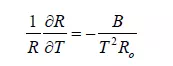
Thermistors (i.e. thermal resistors) are constructed from semiconductors or ceramics which exhibit a strong negative temperature coefficient (“tempco”) (NTC). The temperaturecharacteristic is generally very non-linear. Physically, thermistors come in various shapes and sizes including beads, disks, wafers, rods etc. These are generally encapsulated in glass or resin. Since the conductivity of a piece of semiconductor varies exponentially with temperature,
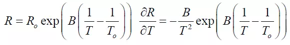
the sensitivity is, consequently:
A related class of passive sensors are a bit more fundamental, appearing pn-junction diodes: The voltage across a biased pn junction is given by where VT is the thermal voltage kT/q. As long as the bias current greatly exceeds the reverse saturation current, which is typically a few fA, The reverse saturation current IS exhibits a strong positive temperature coefficient, and the net
effect is that Vd decreases with increasing temperature (typically −2mV / K , K is the degree Kelvin), making it difficult to use this measurement for precise temperature observation. If,
however, the same diode voltage drop is measured at two different currents, then:
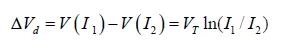
This allows a truly linear measurement of absolute temperature. Alternatively, the two current values may be applied to two identical diodes held at the same temperature, and the voltage
difference can be directly measured.
Hall effect sensors:
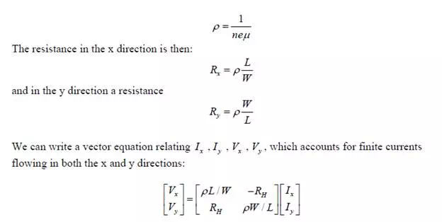
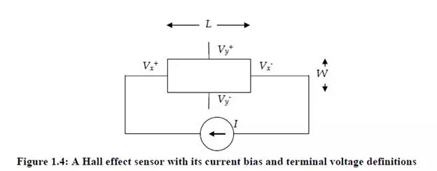
When a current flowing through a rectangular sheet conductor in the x direction is subjected to a magnetic field in the z direction, the electrons experience a force deflecting them sideways and thus producing a voltage across the conductor in the y direction. The Hall voltage measured is proportional to the field strength, and its polarity tells us if the carriers have positive or negative charge (i.e. if they are electrons or holes!). The Hall voltage appears to obey a relation similar to Ohm’s law: H H V = IR , with the Hall resistance H R given
by:
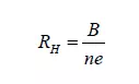
where n is the sheet carrier density and e the electron charge. At the same time, the ribbon, of sheet carrier density n and electron mobility μ has a resistivity of:
Since the Hall resistance is inversely proportional to the carrier density, Hall probes are usually made as thin strips of low carrier density semiconductors, or even true 2-dimentional sheets of
electrons residing at heterostructure interfaces. Examples are the MOSFET inversion layer and the (Quantum well) channel of HEMT (High Electron Mobility Transistors). The Hall Effect is
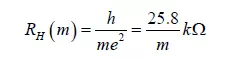
also used to measure carrier densities in materials. At very high magnetic fields and very low carrier densities and temperatures, a Hall probe may exhibit the Quantum Hall Effect in which the Hall resistance is quantised to integral submultiples of a fundamental constant (m is an integer):
Even more fascinating is the fact that the longitudinal resistance vanishes at the values of the magnetic field where the Hall resistance is quantised. It is superficially surprising that the
longitudinal conductance also vanishes at these field values. However this surprising result follows by simply inverting the resistance matrix. The Quantum Hall Effect measurement is
reproducible between differently constructed samples. It is a reproducible SI standard for the resistance measurement. The Quantum Hall Effect is used as a primary standard in Standards
offices for production of secondary calibration standards for resistance meters.
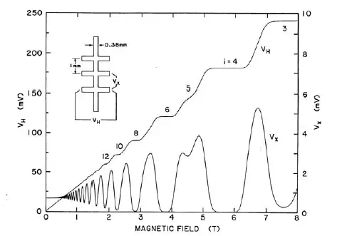
Figure 1.5: The quantum Hall Effect.


Comments are closed.