Collimated and Ionized Metal Plasma (IMP):
There are some more advanced techniques in the PVD. One is called collimated PVD. Another is called ionized metal plasma or IMP PVD. During deposition, we want uniform deposition on the wafer. i.e. the deposited film thickness must be the same at the centre of the wafer, at the edge of the wafer and anywhere in-between. If the target is very small compared to the wafer, it will look like a point source for the deposited material. In that case, the wafer centre will have higher deposition and the wafer edge will have lower deposition.
- One way to improve this is to increase the target size. If the target is large, then the deposition will be uniform. In that case, the target can be near the wafer and still we can get uniform deposition.
- On the other hand, we can pull the target away. If it is too far away, then most of the wafer will be more or less at the same distance from the target and hence, the deposition will be uniform. This is called “long throw”.
- Additionally, the wafers can be rotated during the process, and this also helps in obtaining uniform film thickness.
However if we increase the target distance, then the chamber will become very large and to evacuate the chamber and operate, one will spend correspondingly high energy. The goal of uniform deposition can be achieved by another method called collimated beam. A schematic is shown in the figure 3.11.
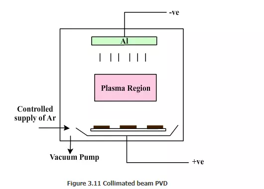
In this, a plate with holes is placed between the target and the wafers. The target atoms, which are coming towards the wafer, will have to come in straight line. Only then they will pass through the collimated plate. Otherwise, they will be stopped by the plate. This ensures that all of them are coming at similar angle and the film deposited will be uniform.
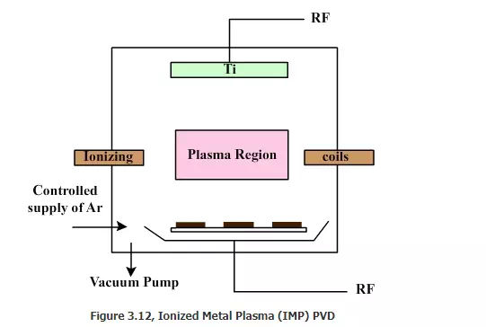
The most advanced method to obtain uniform thickness is called ionized metal plasma or IMP. A schematic of the IMP sputtering equipment is shown in figure 3.12. In this, the metal clusters that are coming towards the wafers are ionized using ionizing coils. Thus the titanium or aluminum metal atoms that are coming are ionized. They become charged and they will be attracted towards the wafer. Hence, even if they start at a different angle when they ejected out of the target, they will all move vertically towards the wafer because of the attractive forces. Since they are all coming at similar angles, the deposition will be uniform. The best quality of the film is obtained when IMP sputtering is used. In the next section we will look into the second deposition technique, viz. CVD.
Chemical Vapor Deposition
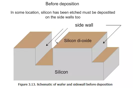
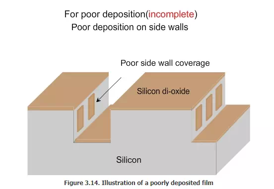
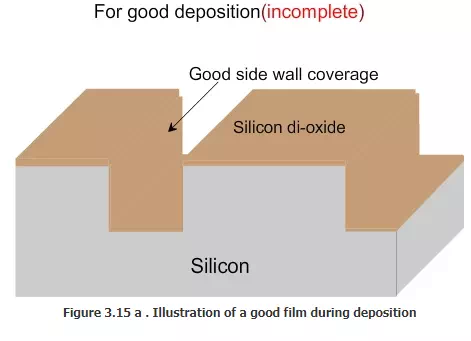
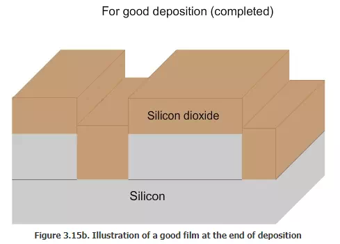
In the PVD method described above, it is not easy to deposit a material on the side walls as shown in fig 3.13. This is especially true if the depth is very high and the opening si small. If the ratio of diameter (or width) to the depth, known as aspect ratio, is very high, PVD cannot give a good side wall coverage (Figure 3.14). However, CVD can be used to get a good side wall coverage (Figure 3.15).
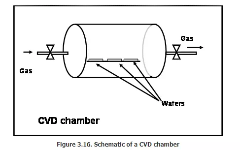
A large CVD chamber may be of 6 ft long and 3 ft diameter. In this, a material may be deposited on a lot (i.e. a batch) of 25 wafers. The CVD chamber will have pipes and automatic valves to create vacuum and to supply desired gases at controlled rates. The material to be deposited (e.g. tungsten) will be in the form of a compound, in the gaseous form. The CVD chamber will also have facilities to heat the wafers in a controlled fashion. A simple schematic of a CVD chamber is given in Figure 3.16
Operation:
First the wafers are kept in the chamber and the chamber is evacuated. Then the wafers will be heated to the desired temperature. Next the gases are supplied and they react only on the surface of the wafer and deposit the material. For example, let us assume that we want to deposit tungsten on the wafer. For this, a mixture of tungsten hexa fluoride, hydrogen and nitrogen (all in gaseous form) will be supplied to the chamber at low pressure. The temperature of the wafer would be maintained between 150 to 300 oC. In the CVD technology, the phrase “high temperature” refers to 800+ oC and low temperature may refer to “less than 400 oC”. Very low temperature may refer to room temperature.In most of the CVD tools, all the chamber walls will be maintained at relatively lower temperature compared to the wafer. Only the wafers would be heated. WF6 and H2 will react only at high temperature. Hence the reaction will occur only on the wafer and not on the chamber walls. This type of CVD process is called low pressure CVD or LPCVD. Using this method many materials such as W, Ti, TiN, Cu, SiO2, Si3N4, Si etc can be deposited on wafer. The side wall coverage will also be good. Some example reactions to deposit various materials are given below.
1. To deposit silicon
SiCl4 + 2 H2 → Si + 4 HCl
SiH4 → Si + 2H2
2. To deposit poly silicon
SiH4 → Si + 2H2
3. To deposit silicon di oxide
SiH4 + O2 → SiO2 + 2H2
SiH4 + 2N2O → SiO2 + 2N2 + 2H2
SiH2Cl2 + 2 N2O → SiO2 + 2N2 + 2HCl
4. To deposit Silicon nitride
3 SiCl2H2 + 4 NH2 → Si2N2 + 6H2+ 6 HCl
SiH2 + NH2 → SixNyHz+ H2 (some hydrogen is incorporated in the film)
5. To deposit Tungsten
WF2 + 3 Si → 2W + 3 SiF4
WF6 + 3 H2 → W + 6HF
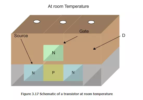
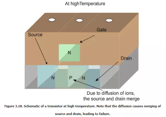
There are certain disadvantages associated with the CVD process. Many of the gases used in CVD and highly corrosive and toxic. Hence good safety measures need to be taken. Also, the cost of the high purity chemicals is also high. If the temperature and pressure are not controlled well, the reaction will occur in air itself and form tungsten (or whatever we are trying to deposit). These tungsten will appear like a dust and will fall on wafer. This dust particle will not stick well to the wafer and will degrade the deposited film quality. The temperature cannot be raised arbitrarily during chip manufacturing. This is because a transistor is made with impurities doped in particular location. When the silicon wafer is heated, the dopants will move and the transistor will not function properly as shown in Figure 3.17 and Figure 3.18 . To avoid this, the wafer must not be heated. Then how do we deposit the material? Plasma comes to help here.
If the WF6 and other gases are passed while a high electric voltage is applied in the chamber, plasma will form. This is similar to creating plasma in PVD. Now the reaction will occur even at low temperature. This type of CVD is called Plasma Enhanced CVD or PE-CVD. In this method, high magnetic field can be applied to increase the density of plasma and improve the deposited film quality. This process is called High Denisty Plasma CVD or HDP-CVD. We saw the materials such as silicon dioxide can be deposited using CVD. For example, Tetra Ethyl Oxy Silane (TEOS) can be heated to high temperature (or disintegrate in presence of plasma) and form silicon dioxide. Similarly silane gas (SiH4) and ammonia will react to form silicon nitride. These films would be called as LP nitride, PE-nitride or HDP-nitride depending on the method used to deposit them.
Comments are closed.