In dry etching, chemical reaction occurs between the material on the wafer and the gases. In this method, the products of the reaction must be gaseous. Otherwise, the product will remain on the wafer. Gases can etch only a few materials in the normal state. However, if we create plasma in the etching chamber, the gas molecules will split into ions, atoms and radicals. These are highly reactive and will react with almost any material.
For example, if the silicon or silicon dioxide on top of the wafer has to be etched, carbon tetra fluoride (![]() ) and hydrogen (
) and hydrogen (![]() ) gases can be used. The wafer will be held in an etching chamber, which also has plates with electrical connections. First the chamber will be evacuated and then
) gases can be used. The wafer will be held in an etching chamber, which also has plates with electrical connections. First the chamber will be evacuated and then ![]() and
and ![]() will be fed into the chamber at a slow rate (a few g/s). They will NOT react with silicon or silicon dioxide. If the plates are given high voltage, a plasma will form and this will split the gas molecules into
will be fed into the chamber at a slow rate (a few g/s). They will NOT react with silicon or silicon dioxide. If the plates are given high voltage, a plasma will form and this will split the gas molecules into ![]() +, F, CF2+, H etc. These ions and radicals can react with silicon or silicon dioxide and etch them away.
+, F, CF2+, H etc. These ions and radicals can react with silicon or silicon dioxide and etch them away.
An example of radical generation in presence of plasma is given below![]()
The fluorine radicals and the ![]() radicals generated are very reactive. They can react with silicon di oxide and form silicon tetra fluoride, which is a gaseous product.
radicals generated are very reactive. They can react with silicon di oxide and form silicon tetra fluoride, which is a gaseous product.![]()
![]()
They also react with silicon to form silicon tetra fluoride![]()
![]()
Note that carbon monoxide, carbon and oxygen radicals are also formed as byproducts. The actual number of reactions occurring during dry etch is very high, but only the main reactions are given here for the sake of simplicity. The reaction rate of silicon with fluoride ion is much more than the reaction rate of silicon dioxide with fluoride ion. In presence of hydrogen, the fluorine radicals combine with hydrogen radicals as shown below. This reduces the availability of fluorine radicals. If we want to remove silicon dioxide, but not silicon, then we have to send more of hydrogen and less of On the other hand, if in presence of oxygen, the availability of fluorine radicals will increase due to the following reaction If we want to remove silicon and not silicon dioxide, we have to send ![]() and oxygen, instead of hydrogen. Thus it is possible to control the removal rate of silicon di oxide and silicon by suitably adjusting the feed gas concentrations.
and oxygen, instead of hydrogen. Thus it is possible to control the removal rate of silicon di oxide and silicon by suitably adjusting the feed gas concentrations.
Whatever may be the gas, if the voltage applied to the plates is removed, the plasma will disappear and the etching will stop. This is one major advantage of dry etching. We can start and stop the etching in a very short period of time. In case of wet etching, even if we take the wafer out of the bath, some of the chemicals will be on the surface of the wafer and will continue to etch the material until it is thoroughly washed and all the chemicals are removed.
One of the issues that can arise during etch is called microloading. Since the dry etch is conducted at low pressure, the concentration of reacting species will not be high. If a certain region has either a large trench or many small trenches, then that region will utilize most of the reactants in that area. Hence the etch rate will be normal in the beginning but will tend to decrease after some time. In other areas, where only small trenches need to be etched, only part of the reactants would be consumed at that time. Hence the etch rate will not decrease in those areas even after some time. Thus, there is a non uniformity in the average etch rate, depending on the ‘aerial density’ as viewed in the layout. This local variation in etch rate, due to the local depletion of reactants is called micro loading. In some fabs, while optical proximity correction (OPC) is implemented during mask making to account for the non-idealities in lithography, corrections are also implemented to account for micro loading. i.e. extra dummy structures may be used in areas with low aerial density so that the etch rate is uniform across the chip. This correction, accounting for the etch process and lithography, is called process proximity correction (PPC).
Under etch and over etch:
Let us consider an example to understand the dry etching used in IC manufacturing. Consider the schematic in fig 4.4. Here the copper wire at the bottom must be connected to the higher level. For that, the glass has to be etched at the right place. Then copper must be filled in the hole. We will consider only the etching part here. In the Figure 4.4, a hole needs to be etched or drilled through silicon dioxide, from the top in only one direction. It has to stop exactly at the copper level. If it etches less, it is ‘under etch’ and if it etches more, it is over etch. Both are problematic. If it etches in all directions, that is also a problem.
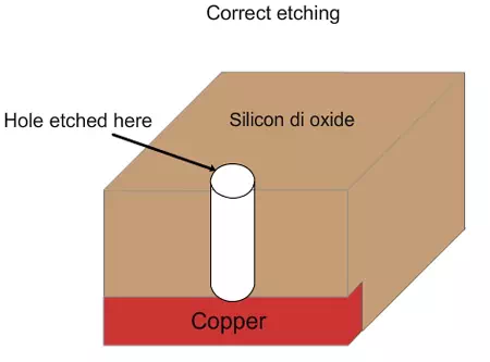
Figure 4.4. Example of correct etch.
In case of under etch, there will be some silicon dioxide left (Figure 4.5). Even if copper is deposited in the hole, it will not connect to the bottom copper line. So, the circuit won’t be complete and the IC will not work.
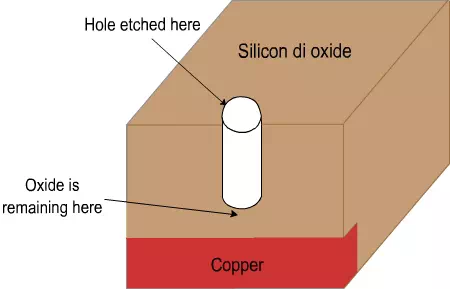
Figure 4.5. Schematic of under etch
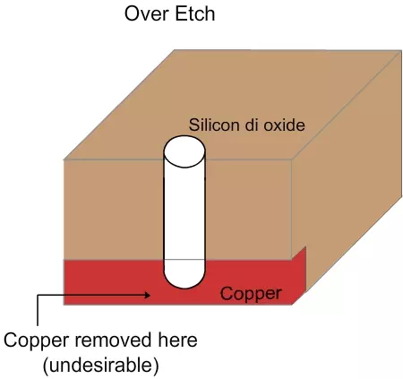
Figure 4.6. Schematic of over etch
In over etch, the copper line at the bottom will get corroded and may even completely disappear (Figure 4.6). This will also lead to the failure of the chip. Also, if the etching happens in all directions, there may be a problem that it will touch a neighboring contact. So, unidirectional etching is essential. Normally, a few wafers will be etched for various times (e.g. 60 seconds, 90 seconds, 120 seconds etc) and the average removal rate would have been calculated based on those. From these values, the etching tool can be operated for a specific time so that the material can be removed up to the desired depth. Even then, there might be some variation in the etching and hence usually the tool is operated for at least 10% longer than the estimate. This is called “over etch”.
If the etching is continued for 10% more time, then won’t it remove the copper at the bottom? Yes, it will. In order to prevent it, there would be a silicon nitride layer on top of copper and below the silicon dioxide, as shown in figure 4.7. The silicon nitride layer will not be easily removed by the chemicals used in silicon dioxide etching. Hence 10% over etch of silicon dioxide will not remove the silicon nitride. After silicon dioxide is etched, the silicon nitride will be etched using dry etching, with different chemicals. Since the silicon nitride layer thickness is very small, the etching time is also very small and it can be etched with good control. Hence the problems due to under etch or over etch will not be there.
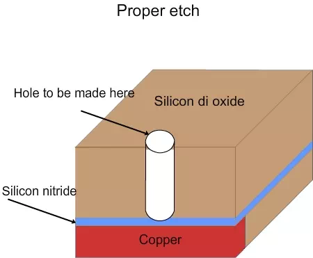
Figure 4.7. Schematic of proper etch using nitride layer in the process flow
Veil and de-veiling: In dry etching, the unidirectional etching is achieved due to two reasons. Since the plasma reacts with the material, heat will be generated. The photo resist will soften a bit and flow down. The flowing film will react with the plasma and form a hard layer, called veil. The veil will not react further with the plasma and will protect the side walls (Figure 4.8 a , b and c). After the completion of etching, the veil has to be removed by using different chemicals, by either wet etching or dry etching. The process of removing the veil is called de-veiling.
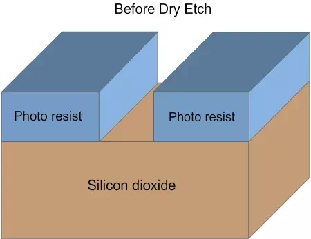
Figure 4.8 a. Schematic of wafer before dry etch
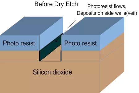
Figure 4.8 b. Schematic of veil formation during dry etch
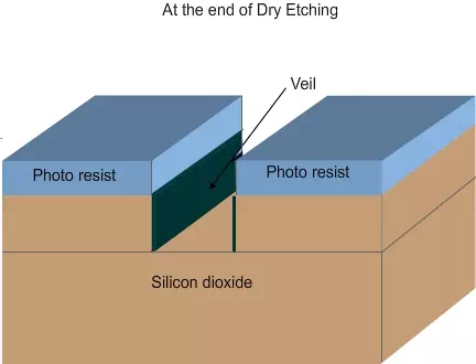
Figure 4.8 c. Schematic of the wafer at the end of dry etch. Note that the veil formation helps in anisotropic etch.
Secondly, the wafer is usually kept near the negative plate which is used for generating the plasma. The positive ions in the plasma will come towards the wafer and sputter away some material. Hence the etching will be unidirectional. This sputtering based removal can be enhanced by adding argon gas. Argon ions will attack the wafer and remove the material (Figure 4.9). However, they will not react with the wafer. The only disadvantage is that argon will attack both the material to be removed (like silicon dioxide) and the photo resist. The other chemicals in the plasma like CF4, H2, O2 can be changed and the removal of silicon or silicon dioxide can be controlled well. But the argon will remove all materials and the selectivity will be lowered. The dry etch without argon is called plasma etching and the one with argon is sometimes called reactive ion etching (RIE), since reacting chemicals as well as argon ions are present in that type of etching. By controlling the argon and other chemicals, it is possible to obtain very good anisotropic etching while maintaining acceptable selectivity.
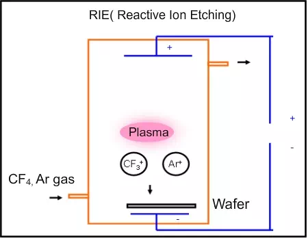
Figure 4.9. Schematic of Reactive Ion Etcher
Using magnetic field, the plasma can be confined to a small region and the density of the plasma can be increased. This is referred to as “high density plasma”. High density plasma will increase the etch rate significantly. It is not practical to use etching for removing excess copper. In wet etching, there is no control and anisotropic etch will be catastrophic. In dry etching, at moderate temperatures, the reaction products are not volatile and hence they do not come out of the wafer. Hence another technique called chemical mechanical planarization or CMP is used for making copper interconnects.
One of the difficulties encountered in dry etching is electrostatic discharge (ESD). When aluminum is used as interconnect material, dry etch is used to remove unwanted aluminum. In the beginning, a continuous layer of aluminum would be present. At later stages, since some aluminum will be etched, islands of aluminum will form and finally the correct structures would be left. In presence of high voltage used for plasma generation, the aluminum islands can acquired charge. They are connected to the transistors at the bottom and if the charge accumulated is high, they can break the gate oxide and destroy the transistor. This is an example of electrostatic discharge (ESD). The charge accumulated is proportional to the area that the aluminum network can form during the process (i.e. the area of any island). During the design phase itself, the maximum area of such island is specified. Since the islands or network act as an antenna during dry etching, this rule is sometimes called as “antenna rule”. To minimize the risk of ESD, certain diodes are used as ‘safety valves’. Note that these diodes do not play any role in the chip design and functioning and are there only to ensure that the process does not destroy the transistor.