Why are the neutral atoms removed from the beam just before deposition? The total quantity of impurities added is measured using the current used for neutralizing the charge. If neutral atoms fall on the wafer, they will not need any electron. Thus the quantity of doping will be calculated incorrectly. Hence the neutral atoms are removed just before doping. The ions falling on the wafer will collide with the silicon atoms and lose momentum. After many collisions, they will come to rest. Depending on the speed of the incoming ions, the location where they stop is determined. The wafer chamber is in high vacuum and this must have very low particle or contamination. The wafer is held with a clamp or electrostatic chuck, which is sometimes called ESC. It will also have anti-static devices in the chamber because the charge measured here is very important. The amount of current needed to neutralize the positive ion is used to calculate how much doping has occurred. If the ion is with 2+ charge, then the total current must be divided by 2 to estimate the amount of deposition. If the top of the wafer has an insulator, then the current will not pass through that significant amount. If it is a semiconductor, the electrons from the back of the wafer can pass through the wafer and neutralize the positively charged ions. If the top is a dielectric then this cannot occur, and with too much charge building upon the dielectric, it may get damaged. In order to avoid this, a flood gun can be used to provide electrons from the front side, thereby neutralizing the positively charged ions, but the amount of electrons supplied must be counted, so that it can be subtracted from the total electron count used for calculating the dosage. We have to remember that we do not want doping in all the places and it is needed only in some places. The places where doping is not needed must be masked. They can be masked with photo resist or with oxide. Photo resist can be used for medium and low energy for moderate doses. For high energy and high doses, photo resist cannot be used because the temperature will increase and the resist will start moving. Sometimes, the resist can also form polymerization, which will make it less soluble for the later steps. So removing the photo resist will be an issue.
Transverse straggle and Channeling:
During diffusion we saw that lateral diffusion is a problem. In implantation also, a similar problem occurs. This is called transverse straggle.
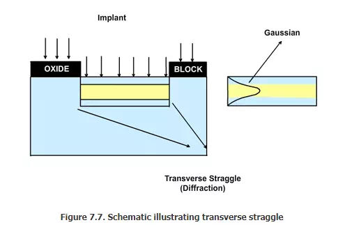
Even though the ions come vertically near the edges, they can bend a little due to diffraction effects and there will be some deposition or doping in the lateral direction. Few other problems also occur in implantation. One is called channeling. Some of the ions will go through the crystal structure very fast and most of them will go through with some resistance offered by the crystals. Most of the atoms will stop at a particular range called projected range with some variation, but the atoms that go through channeling will go far and hence the location of doping will not be controlled well.

Minimization of channeling:
One way to prevent channeling is to hold the wafer at an angle. This can prevent channeling, but it can cause other issues like increase in transverse struggle and also cause shadow as shown in the figure.

Too much of an angle can also be a problem. Another way is to deposit amorphous material on the top. It has to be very thin so that it will not stop the ions, but an amorphous material will make sure that the incoming ion does not see a very uniform structure with gaps.

The third option is, instead of depositing amorphous material, just damage the top of the wafer; that is, make it amorphous using high-energy silicon implant. The fourth choice is to increase the temperature and reduce the channel cross-section.
Rapid thermal annealing : After ion implantation, the Si crystal will have a lot of defects and will have stress. The stress must be relieved and the defects reduced. This process is called ‘repair’. If the wafer is heated and cooled, then these goals can be achieved. However, the dopants will diffuse at high temperature and hence the profile will change significantly. If the wafer is heated quickly, the dopant diffusion is minimized, but the defect and stress levels will reduce. This process is called Rapid Thermal Annealing (RTA). The typical activation energy for repair (5 eV) is more than the typical activation energy for diffusion (3 or 4 eV). Hence, high temperatures favor repair over diffusion. The rapid increase in temperature is achieved by using lamps or lasers, but furnace can be used for relatively low temperatures (<500 ˚C). Heating rates in the range of 100 to 1000 ˚C/s can be achieved. The high temperatures are measured using pyrometers. In case of lamps, tungsten halogen bulbs or arc lamps are used. These operations are conducted in high vacuum. Otherwise, the silicon wafer surface will get oxidized quickly.
Comparison of diffusion and ion implantation: When we compare diffusion versus ion implantation, we should note the following: the deposition plus diffusion process depends on the chemical nature of the species and the solubility. We can never implant more than the solubility limit of the dopant by the diffusion process. In implantation, the doping depends on the energy of the ion beam. We can dope more than the solubility limit. Implantation is more expensive than diffusion. We can control the junction depth, and profile much better than implantation; we can also see or ensure that the maximum concentration of the dopant occurs inside in a specific location, whereas in diffusion, the maximum concentration will always occur on the surface. In the diffusion, the side diffusion is significant in ion implantation even though there is transverse struggle – the movement to the side is relatively less.
Comments are closed.