We saw that material can be deposited on the silicon wafer by various techniques such as PVD, CVD etc. The methods which modify the silicon wafer are also needed for IC manufacturing and they are ion implantation, diffusion and oxidation. We saw the details of diffusion earlier. In this section, we will learn about the ion implantation technique.
Basics:
Silicon, phosphorous and boron and solids. They can be added by diffusion, which is a relatively less expensive process. However, the depth of doping and the quantity of doping is not precisely controllable. Hence the transistor dimensions would not be very precise. When the transistor dimensions were 10 micron (i.e.10,000 nm)or so, if the variability in doping level is 100 nm, it was acceptable because it was only 1%. When the transistor size itself is 100 nm, this much variability is not acceptable. For the ICs with small transistors, ion implantation is used. In ion implantation, the phosphorous (or boron) must be first ionized. Then they must be accelerated and made to impinge on the wafers. Then they will penetrate into the wafer. This is similar to firing bullets into a solid wooden door. The bullets will get embedded into the wood.
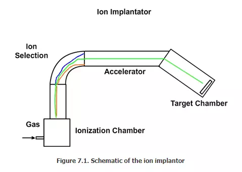
Equipment and operation: Ion implantor will be approximately 10 ft long, 10 ft wide and 10 ft high. A simplified schematic is given in Figure 7.1. We can divide the equipment into four sections as explained below.
- Ionizing chamber
- Ion selection chamber
- Acceleration chamber
- Doping chamber
Ionizing chamber:
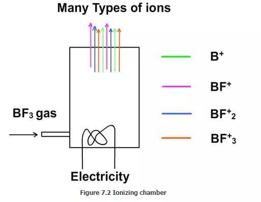
For doping phosphorous, phosphorous pentoxide (P2O5) is used. For doping boron, boron trifluoride (BF3) is used. Phosphrous pentoxide is a solid. It has to be heated and evaporated. BF3 is a gas at normal conditions. Any material used for ion implantation must be brought to gaseous state. Let us assume that BF3 is used for doping. The atoms in BF3 must be converted to ions. In the ionizing chamber, a low pressure is maintained and a tungsten filament is heated using electricity (Figure 7.2). When it is very hot, electrons are emitted from the filament in a process called thermionic emission. Some of the electrons hit the BF3 molecules and create ions such as BF3+, BF2+, BF+ and B+. Thus ions are created from the gas.
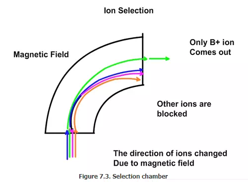
Ion selection chamber: The next section is the selecting chamber. We would like to dope the wafer with boron only and not with fluorine. Hence only B+ must be selected from the mixture of ions and added to the wafer. In order to select the required ion (B+), electric field and magnetic field are used. If we send the stream of ions between two electric plates, which have positive and negative connection as shown in Fig 7.2, the ions will be attracted to the negative plate and move towards the negative plate. If a magnetic field is also applied at the same time, the direction of the movement will change. The speed and the direction of the movement will depend on the charge and the mass of the ions. A plate with a hole in the appropriate place can be used to block all the ions except the desired one (Figure 7.3). Thus B+ ion can be separated from the mixture of ions.
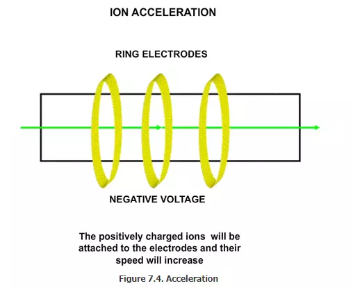
Accelerating chamber; The B+ ions will come with a moderate speed. In order to ensure that they penetrate the wafer, they must be accelerated. For this, a set of ring electrodes are used (Figure 7.4). If negative charge is applied on the plates, the ions will get accelerated considerably. They form what is called as “ion beam”. The ionizing chamber must be kept under high vacuum. If any neutral molecules are there, the boron ion (B+) may hit them and take up an electron and become neutral boron atom (B). We should not dope the wafer with boron atom, but should use only the boron ion. We will see the reason shortly.
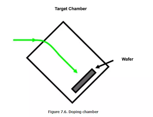
Doping chamber:
In order to ensure that only boron ions are used for doping, just before the beam enters the doping chamber, a magnetic field is used to change the direction of the ion beam. The magnetic field will change the direction of only the ions. The neutral atoms will not be affected by the magnetic field. Thus only the ions will fall on the wafer. The next section is called wafer chamber (Figure 7.6).. The beam size is approximately 1 cm2. The wafer size can be 200 mm or 300 mm. So the beam has to be scanned over the entire wafer. There are two ways of scanning: one is called electrical scanning and the other is mechanical scanning. In the electrical scanning, using electrodes, the beam is moved by applying suitable positive and negative voltages. In the mechanical scanning the wafer is moved, while the beam is held stationary. Sometimes, a combination of beam scan and rotation of wafer is also used to ensure uniformity.
When the boron ion is added to the wafer, the positive charge has to be neutralized. This is done by supplying electrons from the back of the wafer. We can measure the total current used for this and from this calculate the amount of boron deposited. By this method, the exact quantity of boron added can be measured very precisely.
Comments are closed.