Electronic Devices plays an important role in sensors and controllers which are the two eyes of instrumentation and control engineering. So i am slowly going to discuss about the important electronic devices in our blog.
Zener diode is a specially designed PN junction diode. a reverse biased, heavily doped PN junction diode which is operated in the breakdown region is known as zener diode. It is also called a voltage regulator diode or breakdown diode.
Construction of Zener Diode:


Figure 1 shows the symbol of a zener diode. it is similar to the symbol of an ordinary PN junction diode except that its bar is just turned into Z shape. Figure 2 shows a practical equivalent circuit of a zener diode. this circuit shows that a zener diode is equivalent to a battery with voltage (Vz) called zener voltage in series with a resistance (rz) called zener resistance.
Working Principle of Zener Diode:
We will see the working of zener diode as two sections like forward bias and reverse bias.
Forward bias:

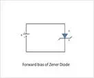
Figure 3 shows the arrangement for forward bias. The positive terminal of the battery is connected to the anode (A) and the negative terminal of the battery is connected to the cathode (K). When applied voltage is zero no current flows through the zener diode. when the forward biasing voltage is increased the potential barrier is reduced and the current starts flowing in the circuit.
Reverse Bias:

Figure 4 shows the arrangement for reverse bias. The negative terminal of a battery is connected to the anode (A) and positive terminal of the battery is connected to cathode (K). the reverse bias operation is explained in VI characteristic.
V-I characteristic of zener diode.

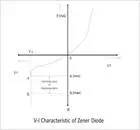
The forward and reverse V-I characteristic shown in the figure 5. The forward current increases slowly upto the knee voltage. Beyond this voltage the current increases sharply with increase in applied voltage. Thus under forward bias condition zener diode acts like an ordinary PN junction diode.
Under reverse bias condition a small reverse current flows through the zener diode. When a reverse voltage across a zener diode is increased, a critical voltage called breakdown voltage is reached at which the reverse current increases sharply as shown by the curve PQ in the figure 5. This breakdown voltage is called zener breakdown voltage or simply zener voltage. This voltage is almost constant over the operating region. This ability of a diode is called regulating ability and is an important feature of a zener diode. It maintains an essentially a constant voltage across its terminal over a specified range of zener current values.
Vz – Zener breakdown voltage.
Iz (min) – A minimum value of zener current called break over current.
Iz (max) – A maximum value of zener current above which the zener diode may be damaged.
Zener break-down
Zener breakdown takes when both sides of the junction are very heavily doped and the depletion layer is thin. When a small reverse voltage is applied a very strong electric field is set up across the thin depletion layer. This electric field is enough to break the covalent bonds. Now extremely large number of free charge carriers are produced which constitute the zener current. This process is known as zener breakdown. In this process the junction is not damaged. The junction regains its original position when the reverse voltage is removed.

Avalanche breakdown
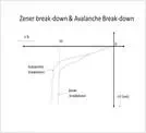
The avalanche breakdown takes place when both sides of the junction are lightly doped and the depletion layer is large. When the reverse bias voltage is increased, the accelerated free electron collides with the semiconductor atoms in the depletion region. Due to the collision with valence electrons, covalent bonds are broken and electron-hole pairs are generated. These new charge carriers so produced acquire energy from applied potential and in turn produced additional carriers. This forms avalanche multiplication. This avalanche multiplication causes the reverse current to increase rapidly. This leads to avalanche breakdown. Once this breakdown occurs the junction cannot regain its original position. This breakdown occurs at higher reverse voltage as shown in the figure 6.
Applications of zener diode.
● It can be used as a voltage regulator.
● It can be used as a limiter in wave shaping circuits.
● It can be used as a fixed reference voltage in transistor biasing circuits.
● It is used for meter protection against damage from accidental over voltage.
● It can be used as a fixed reference voltage in a network for calibrating voltmeters.


