In this chapter we will see various deposition techniques that are used in microelectronic fabrication. If a material like copper or tungsten has to be deposited onto the silicon wafer, there are multiple ways to achieve that goal. The deposition methods used in semiconductor industry can be divided into four groups.
- Physical Vapor Deposition (PVD)
- Chemical Vapor Deposition (CVD)
- Electrochemical Deposition (ECD)
- Spin-on coating
Among these four processes, PVD and spin-on coating are purely physical processes. CVD and ECD are chemical processes. That means in CVD and ECD, chemical reactions occur. In IC manufacturing, the actual quantity of material to be deposited in any single step is very low. The deposited material will be in the form of a thin film, almost like the painting on a surface and in reality much thinner than the paint coating.
Thin film requirements: Any deposition method must satisfy certain requirements:
- The deposition must be uniform throughout the wafer
- A very good control is necessary. If we want 1000 nm of the material deposited on the wafer, then the variation must be within one or two percentage. i.e. the thickness of the film after deposition must be at the minimum 980 nm and at the most 1020 nm.
- In the places where trenches or vias are made, the side wall coverage must be good. This is explained in the later section (figure 3.11)
- The material should adhere to the wafer well and should not peel off
- Dust particles should not fall onto the wafer during the deposition process
- The crystal structure of the film deposited must be of sufficient quality because it will affect the properties of the film. For example, when copper is deposited, we need large grain size since it will result in less electrical resistance.
- If we are depositing alloys, then the composition must be uniform throughout the process
In general, PVD is used to deposit titanium, titanium nitrate, tantalum, tantalum nitrate, aluminum and a very thin film of copper called seed layer. CVD is used to deposit tungsten, titanium, again copper seed layer, silicon di-oxide, silicon nitride, etc. Electrochemical deposition is used for depositing copper. Spin-on coating is used to deposit insulators or dielectric materials, which are usually organic in nature. Historically, some of the metals were evaporated and then the vapor was deposited onto the wafer. The wafer would be kept at lower temperature and the vapor will cool down and form the solid metal. This methods used large amount of energy and had other difficulties. It could not be used for all materials, and particularly for alloys. The material will also deposit on other places like the chamber walls. Hence, it is not currently used for IC manufacturing. If the raw material is taken in gaseous form and the final material is deposited on the wafer after reaction, it is called chemical vapor deposition (CVD). If the material is taken in solid state, but sent as very small particles or atoms and deposited on the wafer without any reaction, it is called physical vapor deposition (PVD). We will first see the details of the PVD.
Physical Vapor Deposition:
DC sputtering
The PVD equipment will be about 4 ft in height and 4 ft in diameter. The material to be deposited (e.g. titanium) will be at the top, as shown in schematic Fig 3.1
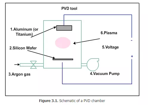
The tungsten will be in the form of a disc of 1 inch thickness and 5 or 6 inches diameter. At the bottom, silicon wafer will be kept. Apart from these, there will be facilities to allow gases into the chamber and to evacuate the chamber with vacuum pump and electrical connections to apply very high voltage (of the order of 10000 V). The negative plate will be near the tungsten and the positive plate will be near the wafer. Tungsten (or any other material in its place) is called target. Why is it called target? How is it deposited onto the wafer? Let us consider an example. In old houses, if we stand inside the house and throw a ball at the top of the house, some of the dust material will fall on the floor. If we throw the ball repeatedly, after some time, the whole floor will be covered with dust. Some dust particles may be coarse and may not stick well to the floor. The fine dust particles will stick well to the floor. In PVD, we can visualize a similar process: Instead of the ball, argon ions are used. The ceiling represents the tungsten target. When the ions hit the target, a few atoms will break away from the target and fall on the wafer. This is a very simplified description of PVD process. PVD is also called sputtering.
First the air in the chamber must be removed and vacuum must be created. Then argon gas sent inside and a low pressure will be maintained. If high voltage is applied to the plates, a plasma will be generated. The plasma will have electrons and positive argon ions. The plasma cannot be generated by normal 230 volts. The positive argon ions will be attracted towards the negative plate. They will move towards the negative plates and hit the tungsten with high force. That is why tungsten is called target in this process.
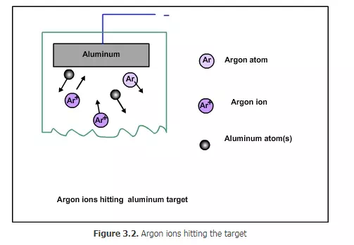
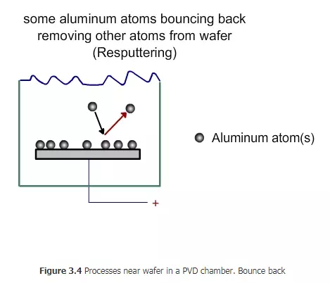
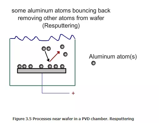
Since the argon ions impinge on the target with large force, some of the target atoms will break and come out , as shown in Fig 3.2. How many tungsten atoms will come for each argon ion hitting the target? This number is called sputtering yield. It depends on the speed of the argon ions, the angle of the impact and also on the bond strength of the target. Tungsten is one of the hard materials. If a relatively soft material such as copper is used as target, then the yield will be higher. The atoms from the target will come towards the wafer with some force. Not all of them will deposit on the wafer. Some will be deposited (Figure 3. 3), while some will bounce back (Figure 3.4). Some may even bounce back and remove some of the materials already deposited on the wafer (Figure 3.5)

Among the tungsten atoms that fall on the wafer, the fraction that stick to the wafer is called sticking coefficient. If all the atoms that fall on the wafer stick to it, then the sticking coefficient is one. If none of them stick, then the sticking coefficient is zero. Typically, the sticking coefficient is about 0.7 to 0.8. ertain techniques are used to ensure that the deposition is uniform. The wafer can be rotated slowly. If the wafer is heated, then the deposited layer can soften and move and also stick well. What is the advantage of using argon to hit the target and deposit the material on the wafer? Why not just use evaporation? Materials such as tungsten have very high melting point (3422 oC) and boiling points (5555 oC). It will be very difficult and energy intensive to deposit tungsten by evaporation. Besides, if an alloy has to be deposited, the composition of the vapor will not be the same as that of alloy. Materials with low boiling point will tend to evaporate early. However, in PVD, since the material is removed by the bombardment of argon ions, the operation can be conducted at relatively low temperature. Alloys can be deposited with out difficulty.
Why do we have to use argon? Argon is an inert gas which will not react with the target or the wafer surface. If we use oxygen or nitrogen instead, they may react with the target and or the wafer surface. We can use other inert gases such as helium or neon. However, it is more difficult to ionize helium or neon. They are also more expensive than argon. Hence argon is used for sputtering. PVD can be used for depositing tungsten, titanium, tantalum, copper, Titanium nitride and tantalum nitride. Currently titanium and tantalum metals and their nitrides are deposited using PVD. Tungsten is deposited using chemical vapor deposition or CVD. A thin layer of copper, called seed layer, is deposited using PVD while the remaining copper is deposited using electrochemical deposition.
RF sputtering:
All the materials we saw above are electrical conductors. PVD can be modified so that insulators such as silicon dioxide or silicon nitride can also be deposited.

What is the problem in using regular PVD for depositing an insulator like silicon dioxide?
Let us look into the figure 3.6. This explains the problem in using the normal PVD chamber to deposit and insulator like silicon dioxide. In the beginning, argon ions will come and hit the silicon dioxide and some of the silicon dioxide will be removed from there and deposited on the wafer. But, the argon will get stuck on the silicon dioxide. Since it is an insulator, the charge will not be removed. The silicon dioxide will acquire a positive charge. The backside of the glass will have negative charge, but there will not be any electrical conduction. Very soon, the entire surface will be positively charged and argon ions, which are also positively charged, cannot approach the glass. The argon ions will not be able to hit the target and deposit the target material on the wafer. If we were using a metal, then the positive charge will be neutralized because the metal will conduct the electron from the backside to the plasma side.
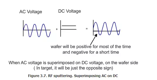
In order to deposit the insulator by PVD, electrons must be supplied to the surface of the insulator on a regular basis. This is achieved by using radio frequency (RF) AC voltage. This is sometimes called as RF sputtering. How does the RF PVD function? The chamber, which uses RF sputtering, looks very similar to the one with normal sputtering, but the voltage applied will be different in this case. This is explained in the schematics shown in figure 3.7 and 3.8. If we take an AC voltage and add it to a DC voltage, then we will get a combined voltage as shown in this figure. If we apply only a pure AC voltage, then 50% of the time the wafer will be positive and 50% of the time the target will be positive. But when we apply the combined DC plus AC voltage, the wafer will be positive 75% of the time and the target will be negative for most of the time. For a short time, the target will be positive and the wafer will be negative.
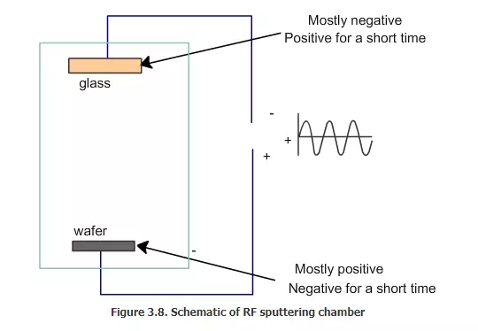
What is the use of this? What will happen when this RF AC voltage is applied along with the DC? When the target is mostly negative, argon ions will come and hit it. Some of the electrons will go and hit the wafer. The glass will be removed by the argon ion and they will go and deposit on the wafer. For a short time, the electrode will be positive near the target; that time the electrons in the plasma will be attracted to the target. They will hit the target. The target has argon ions and the electrons will go and neutralize the argon ions, as shown in Fig. 3.9. Hence, the target will become neutral. Essentially, the electrons are supplied to the target surface from the plasma side and not from the electrical contact at the back.
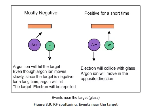
Now will the argon ions go and hit the wafer in the same time? Because argon is much more heavier than electron, and because the duration is very short, it will not hit the wafer that much. Since the electrons are very light (low mass), they will not cause any damage and no atom will be taken out because of the electrons.
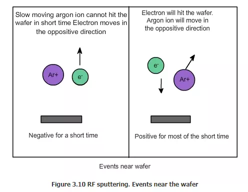
We saw that argon ions will not hit the wafer because it’s for a shorter duration. Even if they hit, they will hit with less force and few hits will occur. In the beginning, in fact, the wafer will be made negative and the target will be made positive. Because of this, the argon will hit the wafer a little, and remove some material and make it rough. This actually facilitates good deposition of the material in the later stages. The initial roughening of the wafer will also help in cleaning any of the contaminant deposited on the material before this process. Now the AC has to be applied at a very high frequency. That is why it is called RF or radio frequency. Now almost all of the sputtering equipment are RF sputtering equipment.