In the previous chapter, we saw that the silicon should be changed to “N” type or “P” type by adding dopants. The addition is carried out either by diffusion process or by ion implantation process. In this section, we will learn about the diffusion process. In general, diffusion refers to the movement of atoms or molecules. However, in semiconductor processing, the term “diffusion” usually refers to the entire process of adding a dopant to the surface of wafer at high temperature. At first, we will learn certain terminologies: What is a junction? How does diffusivity change with temperature? What are the different types of diffusions in solid substrate? Then we will learn about the mathematical modeling of two particular cases of diffusion processes employed in IC industry. Next, we will learn about the type of equipment used for this process. Then we will learn about some of the problems associated with the processes and the ways to resolve them. Finally, we will introduce the idea of sheet resistance and its utility in IC manufacturing.
Junction:
The silicon used for making the ICs is rarely without any dopant, and it usually contains a specific quantity of boron. i.e. it is P-type silicon to begin with. The B atoms are distributed uniformly and hence the doping profile will be uniform. Additionally during chip manufacturing process, dopants will be added by diffusion or ion implantation from the top surface of the wafer. Hence, the concentration profile of the newly added materials will not be uniform from the top of the wafer to the bottom. A schematic illustrates the same.
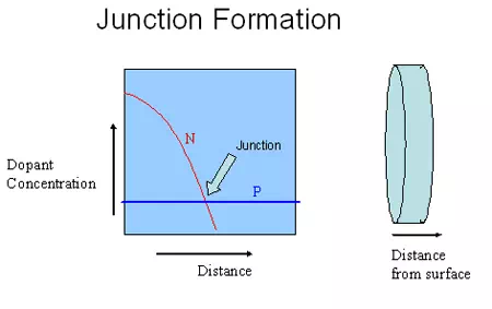
Figure 6.1. Schematic illustration the location of a junction
The expanded version shows that the N type dopant concentration is high on the surface and decreases as we go inside the wafer. At some location, the concentration of N and P type dopants would be equal and that is called the junction. A more precise definition is, “the location where the concentration of electrons and holes are equal is called the junction”. In most cases, the concentration of electrons and holes are given reasonably well by the concentration of N and P type dopants respectively. If the dopants are introduced by the diffusion process, then the surface concentration of those dopants will always be higher than the concentration inside, since the atoms diffuse from high concentration region to low concentration region.
Diffusivity vs Temperature:
At room temperature, the inter-solid diffusivity is quite low and for all practical purposes the atoms can be considered as immobile. The typical temperatures employed are 900 to 1200 oC. The diffusivity in solid state is related to the temperature by Arrhenius equation ![]() where D0 is the pre-exponent and EA is the activation energy. This is valid for solid-solid diffusion. It may be worth mentioning that, for gases, the dependence of diffusivity on temperature is given by
where D0 is the pre-exponent and EA is the activation energy. This is valid for solid-solid diffusion. It may be worth mentioning that, for gases, the dependence of diffusivity on temperature is given by ![]() . Hence, the inter-solid diffusivity coefficient will increase significantly with an increase in the temperature.
. Hence, the inter-solid diffusivity coefficient will increase significantly with an increase in the temperature.
Types of diffusion:
The inter-solid diffusion can occur by two types of movements: 1. substitutional and 2. interstitial. In the substitutional movement, the dopant atom occupies the crystal lattice space normally occupied by the silicon. Hence, it can move from one location to another only if vacant sites are present. In this, it has to break old bonds and form new bonds for each movement and this is inherently a slow process. Elements such as B, P, Ga, As, In and Al diffuse primarily through substitutional mechanism.
ig 6.2 Animation showing (a) substitutional diffusion and (b) interstitial diffusion
In the interstitial diffusion, the dopant atoms are found in the space between the regular crystal lattice sites. Some elements such as Au, Cu, Fe, Na and Li diffuse primarily by interstitial diffusion. They do not form strong bond with the silicon atoms and do not need vacancies to move. Thus, interstitial diffusion is a relatively fast process. Since it is a fast process, it is difficult to control it
Mathematical Modeling of diffusion:
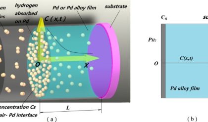
Assuming that the diffusivities are independent of concentration, the relationship between the concentration of dopant (C) at any location (x) inside the wafer at any given time (t) is given by the following differential equation.![]()
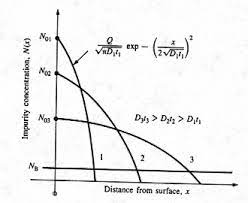
This is the simplified form of the equation called Fick’s second law, which describes the transient diffusion phenomenon. In order to solve this equation, the appropriate boundary conditions must be given. There are two simplified cases that are applicable for diffusion in IC manufacturing. In one case, the concentration of the dopant is always maintained at the surface of the wafer. Inside the wafer, the concentration will change with time. This case is called “constant source” case. In the second case, the total quantity of doptant introduced is maintained constant, but the concentration of the dopant (at all locations, including the surface) will change with time. This is called “limited source” case.
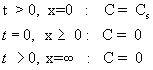
Constant source diffusion: Here, the concentration on the wafer surface is always equal to the solubility limit (Cs). The concentration at a location too far away from the surface (inside the wafer) is zero. Before the beginning of diffusion process, the concentration of dopant in the wafer is zero. These are written as
Sometimes this is also referred to as pre-deposition diffusion, because in those cases, diffusion will be done in two steps. The first step is called pre-deposition and the second step is called drive-in deposition. In the first step, a small quantity of impurity will be doped using the constant source mode and then the source will be removed. In the second step, the wafer will be maintained at high temperature for a certain time. The doped impurity will serve as the source and diffuse further in. Hence the first step is called the pre-deposition diffusion and the second step is called the drive-in diffusion. For the constant source diffusion, the differential equation can be solved as follows.
Use the transformation ![]()
This leads to the following equation.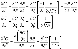
The original equation becomes ![]()
The three boundary conditions reduce to two boundary conditions in the new variable ![]()
Let ![]() . Then the above equation can be integrated as
. Then the above equation can be integrated as ![]()
This is integrated again to give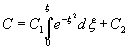
Here C1 and C2 are integration constants.
Using the boundary conditions, we get , C2=Cs and ![]()
Complementary error function is defined as ![]() ,
,
Thus, ![]()