Etching PCB is to use the materials of chemical reactions or physical impact of technologies that are removed. Etching techniques can be divided into wet etching and dry etching, chemical solution used in wet etching through chemical reactions in order to achieve the purpose of etching, dry etching is usually a plasma etching, its effect may be the impact chips by plasma surface physics, or possibly a plasma activated chemical reaction between base and surface atoms, or even role may be a composite of the two.
Wafer Etching
In the semiconductor manufacturing process, often needed in defining the tiny size of the pattern on the wafer, and their formation can be completed through etching techniques. Early used in the semiconductor manufacturing process etching method for wet etching, mostly borrowed from the chemical reaction between solution and etch materials, through available resources and selecting the appropriate chemical solution, given the etch rate and etch materials and light resistance and good etching than lower material. But as integrated circuit component size is getting smaller, because the chemical reaction is not directional, and wet etching is isotropic, when vertical etching the etching solution, at this time, lateral etching will occur simultaneously, and thus undercut phenomenon, resulting in distortion pattern line width. Wet etching in submicron components (3 Micron) has been replaced by dry etching process. Several common substances in the semiconductor manufacturing process of wet etching silicon, silicon dioxide, Silicon nitride and aluminum. Monocrystalline and polycrystalline silicon etching is usually the nitric acid and hydrofluoric acid mixture for, this response is the use of nitric acid oxidation of silicon dioxide on Silicon surface, using hydrofluoric acid will form a Silicon solvent removal, reaction is as follows:
Si + HNO3 + 6HF = H2SiF6 + HNO2 + H2 + H2O
Wet etching of silicon dioxide is usually hydrofluoric acid, reaction is as follows:
SiO2 + 6HF = H2 + SiF6 + 2H2O
Practical application is to use diluted hydrofluoric acid or added fluoride used as a buffering agent to control the etch rate.
Silicon nitride can be heated to 180 ° c phosphoric acid solution (85%) for etching. Wet etching of aluminum or aluminum alloy is the use of phosphoric acid, nitric acid, acetic acid and water mixture, typical for 80% phosphoric acid, 5% nitric acid, acetic acid and 10% water. By nitric acid oxidation of aluminum to aluminum, and then will be dissolving alumina phosphate removal, and so forth to achieve the effect of circuit board etching.
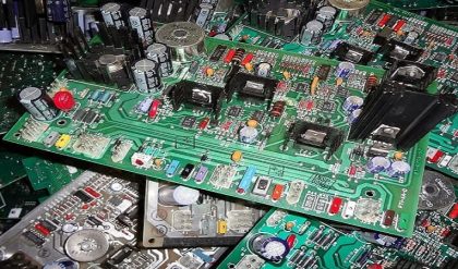
PCB Etching
Currently used for print circuit board etching of solvents are iron (Ferric Chloride), cupric chloride (Cupric Chloride), alkaline ammonia (Alkaline Ammonia), sulfuric acid hydrogen peroxide (Sulfuric Acid + Hydrogen Peroxide) etching fluid, ammonium persulfate, sulfuric acid – chromic acid etching solution. Like the PCB manufacturing in Fusion PCB of Seeed.
Etching liquid are mainly copper chloride solution, ferric chloride liquid, alkaline etching, acid/hydrogen peroxide (hydrogen peroxide) etching. Chloride copper etched liquid by chloride copper (CuCl2 Castle, 2H2O) + hydrochloride (HCl) + hydrogen peroxide (H2O2) + water (H2O) composition; three ferric chloride etched liquid is by three ferric chloride (FeCl3) + hydrochloride (HCl) + water (H2O) composition of; alkaline etched liquid of main components has copper ammonia complex ion; sulfuric acid/hydrogen peroxide (hydrogen peroxide) etched liquid to sulfuric acid and hydrogen peroxide (hydrogen peroxide) mainly components. PCB etching process and copper chloride and ferric chloride market, PCB manufacturers some 95% using copper chloride (CuCl2), IC substrate maker about 80% using ferric chloride (FeCl3), 20% using copper chloride (CuCl2). You can try etching PCB at home.