X-ray lithography uses collimated x-rays as the exposing energy. Being much shorter in wavelength than light, even DUV light, x-rays provide increased lateral resolution. For micromanufacturing though, it is the penetrating power of the x-rays deep into the photoresist that is used. This allows microstructures with great height to be fabricated, relative to optical lithography. It should be noted that the terms “great height” and “high aspect ratio” are often used without specific numbers being applied. As technology progresses, the absolute numbers associated with these terms change. For example, optical lithography has been used to create structures as high as 1 millimeter in newer negative photoresists. One millimeter was generally regarded as a height only attainable with x-ray lithography. Because x-rays interact with matter differently than optical wavelengths, the lithography process uses different materials. The typical x-ray absorber is gold, but most materials with a high atomic number will have a high x-ray coefficient. This is dependent on the wavelength of the x-rays however. The mask substrate is normally a low atomic number material such as diamond, beryllium, or polyimide, or a thin membrane of a higher atomic number material such as silicon or silicon carbide. The substrate is, again, any structural material which fits the particular application and the photoresist of choice is polymethyl methacrylate (PMMA).
Depending on the thickness of the exposure desired, the PMMA is either spun on as a single layer, as multiple layers, or adhered as a pre-cast commercial sheet. The sheet is commonly adhered to the substrate by the liquid monomer, MMA. The thickness of the mask absorber depends on the energy of the x-rays used to make the exposure. For x-rays with an energy in the range of 5 keV (corresponding to an exposure depth into PMMA of several hundred micrometers) from a “ring” (synchrotron) operating at a critical energy of 0.8 – 1.0 GeV, the gold mask absorber must be approximately 5 to 10 micrometers thick to provide good contrast. As the x-ray energy increases, to 35 keV for example (corresponding to an exposure depth into PMMA of several millimeters, or more) from a ring operating at 7 GeV, the gold absorber must as thick as 50 micrometers to provide good contrast between the absorbed and transmitted energy. Again, there are many references available on aspects of this process. X-ray lithography is expensive to perform because of the expense of operating a synchrotron. Depending on what is considered, the cost can run hundreds of dollars per hour just to recover the actual operating expenses without considering the initial investment of tens-of-millions of dollars. Therefore, the LIGA process was developed several decades ago to reduce the dependency on fabrication with a synchrotron.
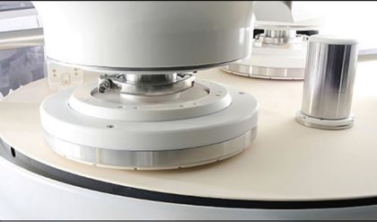
The LIGA acronym is German and stands for in English Lithography-Electroforming-Replication. In the LIGA process, x-ray lithography is used to create a mold in the PMMA resist. The resist is placed on a thin metallic plating base which has been deposited on the structural substrate. The PMMA resist is exposed down to the plating base and, when developed, reveals the plating base. The plating base is used as the cathode in an electroplating process to fabricate a metallic microstructure within the mold. Electroforming is the same as electroplating except the intent is different. Electroplating is generally regarded as a process to protect a surface from corrosion, such as chromium plating, or to provide a decorative surface, as in gold plating. Electroforming implies that the plating is used to create an actual metal component. After electroforming, the metallic negative of the PMMA mold is used as a mold insert for subsequent injection molding or hot embossing. These processes create duplicates of the PMMA mold made previously at the synchrotron. This helps reduce the cost of mass produced microsystems. Examples of micocomponents and microsystems fabricated by x-ray lithography are attached.
