The name optical lithography comes from the early application where the exposing energy was visible light. While those wavelengths can still be used, the push to reduce the size of feature sizes has lead to the use of shorter wavelengths to increase resolution. Ultraviolet (UV) and deep ultraviolet (DUV) sources are now used. Such sources include excimer lasers which operate at wavelengths of 248 nm, 193 nm, and less. Visible wavelengths end in the red at about 400 nm. At these shorter wavelengths, particularly 193 nm, optical materials and even air absorb the energy very well and there are still many problems to be overcome when using this wavelength. The process steps described below are superficial and require advanced levels of technology to be fully effective. There are many references available which more completely describe each process step. The first step in optical lithography is to create a mask. The mask substrate is commonly borosilicate glass or more recently fused-silica because of its lower thermal expansion coefficient and higher transmission at lower wavelengths. The next step is to apply a resist coating to the mask substrate. This is done using a spinner which spins the mask substrate as a small amount on liquid resist is applied at the center. This results in a uniform coating of the liquid resist on the substrate. To mechanically “fix” the resist, it undergoes a prescribed baking operation.
The next step is to pattern the resist with a pattern generator. In photography, the negative is patterned by the scene being photographed. In lithography, the pattern is made by moving a small spot of light over the resist to “write” the desired pattern. The source for traditional optical lithography is a mercury arc lamp which has an output with spectral energy peaks at particular wavelengths. The resist is commonly tailored to be most sensitive at one or more of these wavelengths. For DUV mask patterning, lasers are used. The mask resist may also be patterned by electron beam lithography which can shape the beam to be square or rectangular. The much shorter wavelength of the electrons is one reason for increased resolution using e-beam lithography. After patterning, the mask is developed and a metal coating (commonly chromium) is applied. The chromium fills the voids in the developed resist, as well as on top of the undeveloped resist. The resist is then stripped away leaving a pattern of chromium on the mask substrate. Prior to use, the mask must be inspected, measured, and if necessary repaired.
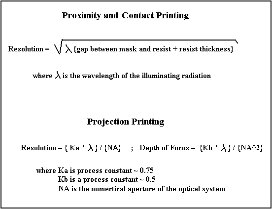
A similar process is performed on the substrate and resist to be patterned for the final structures. For microelectronics, the substrate is silicon or gallium-arsenide. For silicon-based MEMS (microelectromechanical systems), the substrate is also silicon. The mask is then used analagous to a photographic negative and the mask pattern is transferred into the resist carried on the substrate. Normally, the mask is held in very close proximity to the substrate and resist in what is termed proximity or shadow printing. The resolution of the transferred pattern is governed by the diffraction equations for the incident light.
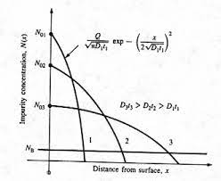
After exposure, the substrate resist is developed similar to the mask resist leaving openings in the resist. This allows access to the substrate for further etching, deposition, or doping. The number of possible subsequent processes is large and will not be repeated here. They are widely available in the open literature, handbooks, and textbooks.