Introduction
Photomasks used for optical lithography contain the pattern of the integrated circuits. The basis is a so called blank: a glass substrate which is coated with a chrome and a resist layer. The resist is sensitive to electron beams and can be transferred into the chrome layer via etch processes. The chrome represents opaque areas on the photomask which are responsible for the casting of shadow during exposure of the silicon wafers. The photomasks are directly exposed with electron beams under hard vacuum. With this method a resolution far below 100 nm is possible. Due to wave optics (e.g. diffraction) there can be aberration during the exposure of wafers. Thus the optical proximity correction (OPC) has been introduced in semiconductor manufacturing, which can eliminate or reduce image defects. OPC means to modify the structures on the mask in such a way that the shape of the image on the wafer looks like desired. Furthermore there can be additional structures just for minimizing aberration which do not have any function for the integrated device itself.
Photomask manufacture
The manufacturing of photomasks is basically equal to the wafer fabrication. The difference is the exposure of the resist which is done by electron beams (photomasks) or with optical lithography (wafer).
1. First step is the exposure of photoresist with electron beams (or laser).

2. Subsequent the resist is developed to form a pattern.

3. The resist acts as a masking to transfer the pattern into the chrome layer by etch processes.

4. Subsequent the resist is removed.

5. Finally a pellicle is montaged on top to prevent contamination of the glass/chrome

Photomasks
Besides the traditional chrome on glass mask (COG) there are various types of photomasks which enhance the optical resolution of the structures. The central issue of COG masks is the diffraction of the light on edges. Thus the light will not only impact in perpendicular direction but will be deflected into areas which must not be exposed.
Spectral intensity of a COG mask
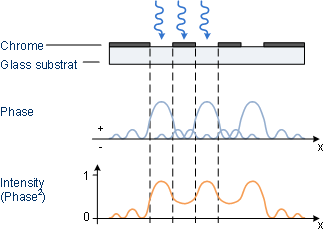
With different means which are described in the following, the intensity of the diffracted light should be reduced.
Attenuated Phase Shift Mask (AttPSM)
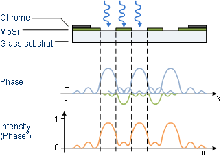
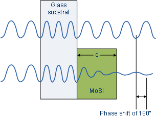
The attenuated phase shift mask (AttPSM; also half tone mask) uses a patterned layer of molybdenum silicide (MoSi) which represents the structures of the circuit. The molybdenum silicide has a thickness which causes a phase shift of the transmitted light of 180°. Thus the phase shifted light and the radiation which transmits through glass only interfere destructively. In addition the molybdenum silicide is dense (6 % or 18 % @ 193 nm wavelength). On the one hand the light is attenuated and on the other hand the light waves which are in opposite phase erase each other almost completely, this results in a higher contrast. A chrome layer can be added to areas which are not used for exposure to mask unused regions. This photomasks are named tritone masks.
Spectral intensity of a Attenuated Phase Shift Mask
Phase shift through molybdenum silicide
Chrome less Phase shift mask
Chrome less phase shift masks don’t use opaque films. The phase shift is achieved by trenches which are directly etched into the glass substrate. The manufacturing of these masks is difficult, since the etch approach has to be stopped in the middle of the glass. In contrast to etch processes where one layer is completely etched till the layer beneath is reached – which causes changes in the etch plasma, so that one knows when the process is finished -, there is no indication when the exact depth in the substrate is reached.
Alternating Phase Shift Mask (AltPSM)
The alternating phase shift mask also uses trenches which are etched into the glass substrate alternating to non-etched areas. In addition there are areas which are covered with a chrome layer to decrease the intensity of radiation in this regions.
Spectral intensity of a Alternating Phase Shift Mask
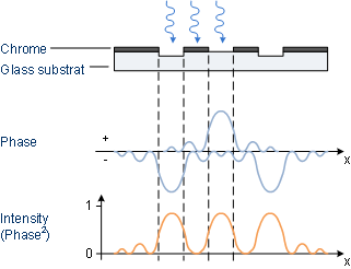
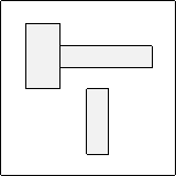
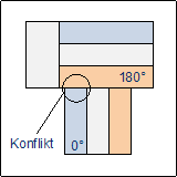
However, there are regions with an undefined phase shift, so that one has to exposure twice with different masks. One mask contains the structures which run in x-direction, while the second mask contains the patterns which are orientated in y-direction.
Desired structures on the wafer and conflict on the mask
Next generation lithography
In the future there has to be a complete change-over which means, that the traditional lithography tools and the photomasks have to be replaced. Next generation lithography is expected to use extreme ultra-violet radiation (EUV, wavelength 13.5 nm) which is absorbed in normal atmosphere as well as in glass. For this reason EUV processes have to take place under vacuum and instead of optical lenses mirrors have to be used for focusing. The photomasks will have a reflective surface instead of translucent glass.
Also beacuse of the tremendous effort (technical as well as of money matters) the traditional lithography is kept alive as long as possible, and new inventions as phase shift masks or immersion lithography have pushed the conventional lithography. Thus today’s feature sizes of only 32 nm can still be exposed with a wavelength of 193 nm. Sometimes there was a thought of the introduction of radioation sources with 155 nm, however, because of the immense costs it is foreseeable that subsequent to argon fluoride lasers (193 nm) EUV sources will be established instantly.
