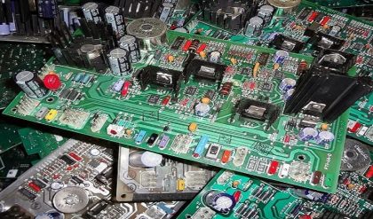
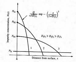
Miniaturization of electronic components and correspondingly the balk and volume of equipments has been an aim which has been progressing concurrently with advance in electronics. This received a tremendous boost with the discovery of transistor in 1948. This simultaneously gave birth to a science and technology called Microelectronics. Microelectronics covers in its ambit not only miniaturization but along with it reliability, high speed, low cost, increased system complexity. Before the advent of integrated circuits, it was the practice to assemble the discrete components as per a planned layout on a metal base and �wire� them. As the base was the major contributor to bulkiness, it was replaced by printed circuit boards (single and double sided). Passive components like resistors and capacitors were created by depositing thin films of metal on a substrate like pyrex and discrete components were plugged at appropriate places and soldered. In the meantime vast improvements were made in the manufacture of the transistors by such processes as epitaxial growth, masked impurity diffusion, oxide growth and oxide etching using photo-lithography for definition. These processes helped in creating on a single-crystal chip of silicon, about 5 mils by 50 mils many circuits of both active and passive components. Hence the name Integrated Circuit IC, in short.
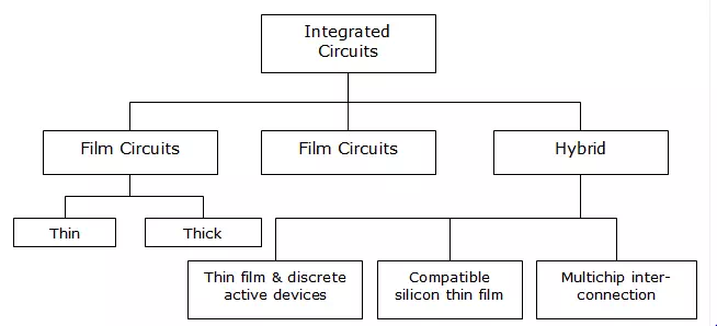
1) Film Circuits consist of layers ofr films of conducting and non-conducting materials on a passive (insulating) substrate like pyrex. In this way passive elements like resistors, inductors and capacitors, are fabricated to high accuracy. By controlling the thickness of the film deposited it can be made thin and thick. FETs are manufactured as thin transistors.
2) Monolithic Integrated Circuits A single wafer of silicon crystal is the substrate on which all the components are made. The wafer is lightly doped P type substrate. The wafer is for 10 cm dia and 10 to 15 units thick(0.2 to 0.3 mm). The single crystal is extremely pure. The wafer is lapped and polished to a mirror finish of 5 units thick approximately. The large piece is then sawed into 100 to 8000 rectangular chips of 1 to 10 mm sides. Each chip is a single IC. A chip may contain an average of 700 components.
Epitaxial Growth On the p type substrate an n type layer, 1 mil (5 to 25 um) thick layer is grown by plcing the wafer in a furnace at 1200C and introducing a gas like phosphine (PH3) for n type doner. Or diborane(B2,H2) for p type acceptor.

The p type substrate has a resistivity of 10 ohm-cm giving Na of 1.4 x 10^15 atoms/cm3. For n layer the resistivity chosen is 0.1 to 0.5 ohm-cm.
Isolation by oxidation
A thin layer of SiO2 is grown on the epitaxial layer. It is 1 micron thick. A photoresist liquid is now coated over the SiO2 layer. This layer will harden on exposure to ultraviolet. A mask, a glass plate with pattern drawn on it, is now placed on the photo resist surface. The mask allows UV light to pass through selected areas and polymerizes(hardens) it. The mask is now removed and the layered substrate washed with a chemical(trichloroethylene) which removes the unexposed portions.
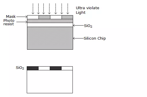
The chip after washing is shown in fig. Then plain areas are the unmasked portion. The chip is immersed in an etching solution of hydrofluoric acid and SiO2 layer is removed. The etching solution does not affect the unmasked polymerized areas. The photoresist is now removed. Completely by scrubbing with heated solvents. P type impurities are now diffused through the silicon turning the n type material into a p type channel extending into the p substrate. The concentration of p type channels is more than that of p type substrate and hence referred as p+.
This process of SiO2 layers, photo resist and masking is repeated for a base collector junction, resistance diffusion etc. The wafer is diced into individual chips. The chip externally small and brittle and is cemented or soldered to gold plated header to which leads are connected. Finally it is hermetically scaled. To-5 can accommodate upto 14 pins.
The number of complete logic gates in a single IC package is described as follows.
- SSI(Small Scale Integration) � up to 10 gates per package
- MSI(Medium Large Scale Integration) � 10 to 100 gates per package
- LSI(Large Scale Integration) � 100 to 1000 gates per package
- VLSI(Very Large Scale Integration) � greater than 1000 gates per package
