When the collector current flows only during the positive half cycle of the input signal, the power amplifier is known as class B power amplifier.
Class B Operation
The biasing of the transistor in class B operation is in such a way that at zero signal condition, there will be no collector current. The operating point is selected to be at collector cut off voltage. So, when the signal is applied, only the positive half cycle is amplified at the output.
The figure below shows the input and output waveforms during class B operation.
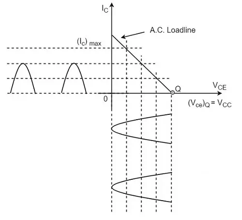
When the signal is applied, the circuit is forward biased for the positive half cycle of the input and hence the collector current flows. But during the negative half cycle of the input, the circuit is reverse biased and the collector current will be absent. Hence only the positive half cycle is amplified at the output. As the negative half cycle is completely absent, the signal distortion will be high. Also, when the applied signal increases, the power dissipation will be more. But when compared to class A power amplifier, the output efficiency is increased. Well, in order to minimize the disadvantages and achieve low distortion, high efficiency and high output power, the push-pull configuration is used in this class B amplifier.
Class B Push-Pull Amplifier
Though the efficiency of class B power amplifier is higher than class A, as only one half cycle of the input is used, the distortion is high. Also, the input power is not completely utilized. In order to compensate these problems, the push-pull configuration is introduced in class B amplifier.
Construction
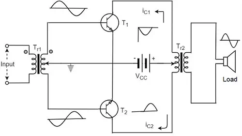
The circuit of a push-pull class B power amplifier consists of two identical transistors T1 and T2 whose bases are connected to the secondary of the center-tapped input transformer Tr1. The emitters are shorted and the collectors are given the VCC supply through the primary of the output transformer Tr2. The circuit arrangement of class B push-pull amplifier, is same as that of class A push-pull amplifier except that the transistors are biased at cut off, instead of using the biasing resistors. The figure below gives the detailing of the construction of a push-pull class B power amplifier.
The circuit operation of class B push pull amplifier is detailed below.
Operation
The circuit of class B push-pull amplifier shown in the above figure clears that both the transformers are center-tapped. When no signal is applied at the input, the transistors T1 and T2 are in cut off condition and hence no collector currents flow. As no current is drawn from VCC, no power is wasted. When input signal is given, it is applied to the input transformer Tr1 which splits the signal into two signals that are 180o out of phase with each other. These two signals are given to the two identical transistors T1 and T2. For the positive half cycle, the base of the transistor T1 becomes positive and collector current flows. At the same time, the transistor T2 has negative half cycle, which throws the transistor T2 into cutoff condition and hence no collector current flows. The waveform is produced as shown in the following figure.
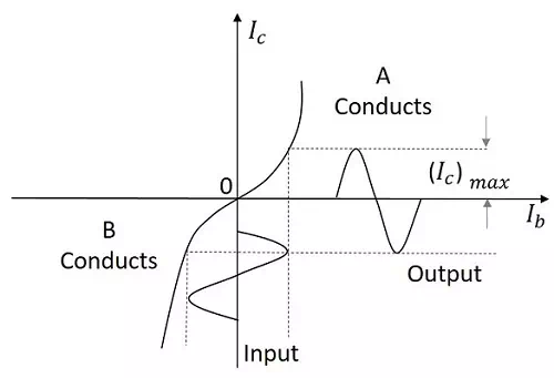
For the next half cycle, the transistor T1 gets into cut off condition and the transistor T2 gets into conduction, to contribute the output. Hence for both the cycles, each transistor conducts alternately. The output transformer Tr3 serves to join the two currents producing an almost undistorted output waveform.
Power Efficiency of Class B Push-Pull Amplifier
The current in each transistor is the average value of half sine loop.
For half sine loop, Idc is given by
Idc=(IC)maxπIdc=(IC)maxπ
Therefore,
(pin)dc=2×[(IC)maxπ×VCC](pin)dc=2×[(IC)maxπ×VCC]
Here factor 2 is introduced as there are two transistors in push-pull amplifier.
R.M.S. value of collector current = (IC)max/2–√(IC)max/2
R.M.S. value of output voltage = VCC/2–√VCC/2
Under ideal conditions of maximum power
Therefore,
(PO)ac=(IC)max2–√×VCC2–√=(IC)max×VCC2(PO)ac=(IC)max2×VCC2=(IC)max×VCC2
Now overall maximum efficiency
ηoverall=(PO)ac(Pin)dcηoverall=(PO)ac(Pin)dc
=(IC)max×VCC2×π2(IC)max×VCC=(IC)max×VCC2×π2(IC)max×VCC
=π4=0.785=78.5%=π4=0.785=78.5%
The collector efficiency would be the same. Hence the class B push-pull amplifier improves the efficiency than the class A push-pull amplifier.
Complementary Symmetry Push-Pull Class B Amplifier
The push pull amplifier which was just discussed improves efficiency but the usage of center-tapped transformers makes the circuit bulky, heavy and costly. To make the circuit simple and to improve the efficiency, the transistors used can be complemented, as shown in the following circuit diagram.
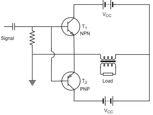
The above circuit employs a NPN transistor and a PNP transistor connected in push pull configuration. When the input signal is applied, during the positive half cycle of the input signal, the NPN transistor conducts and the PNP transistor cuts off. During the negative half cycle, the NPN transistor cuts off and the PNP transistor conducts.
In this way, the NPN transistor amplifies during positive half cycle of the input, while PNP transistor amplifies during negative half cycle of the input. As the transistors are both complement to each other, yet act symmetrically while being connected in push pull configuration of class B, this circuit is termed as Complementary symmetry push pull class B amplifier.
Advantages
The advantages of Complementary symmetry push pull class B amplifier are as follows.
· As there is no need of center tapped transformers, the weight and cost are reduced.
· Equal and opposite input signal voltages are not required.
Disadvantages
The disadvantages of Complementary symmetry push pull class B amplifier are as follows.
· It is difficult to get a pair of transistors (NPN and PNP) that have similar characteristics.
· We require both positive and negative supply voltages.