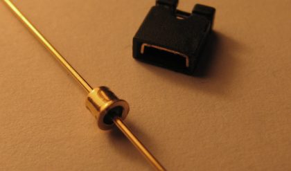
A photodiode is a p-n junction or pin semiconductor device that consumes light energy to generate electric current. It is also sometimes referred as photo-detector, photo-sensor, or light detector. Photodiodes are specially designed to operate in reverse bias condition. Reverse bias means that the p-side of the photodiode is connected to the negative terminal of the battery and n-side is connected to the positive terminal of the battery. Photodiode is very sensitive to light so when light or photons falls on the photodiode it easily converts light into electric current. Solar cell is also known as large area photodiode because it converts solar energy or light energy into electric energy. However, solar cell works only at bright light. The construction and working of photodiode is almost similar to the normal p-n junction diode. PIN (p-type, intrinsic and n-type) structure is mostly used for constructing the photodiode instead of p-n (p-type and n-type) junction structure because PIN structure provide fast response time. PIN photodiodes are mostly used in high-speed applications.
In a normal p-n junction diode, voltage is used as the energy source to generate electric current whereas in photodiodes, both voltage and light are used as energy source to generate electric current.
Photodiode symbol
The symbol of photodiode is similar to the normal p-n junction diode except that it contains arrows striking the diode. The arrows striking the diode represent light or photons.
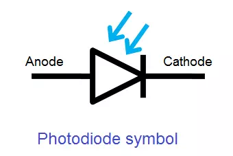
A photodiode has two terminals: a cathode and an anode.
Objectives and limitations of photodiode
- Photodiode should be always operated in reverse bias condition.
- Applied reverse bias voltage should be low.
- Generate low noise
- High gain
- High response speed
- High sensitivity to light
- Low sensitivity to temperature
- Low cost
- Small size
- Long lifetime
How photodiode works?
A normal p-n junction diode allows a small amount of electric current under reverse bias condition. To increase the electric current under reverse bias condition, we need to generate more minority carriers. The external reverse voltage applied to the p-n junction diode will supply energy to the minority carriers but not increase the population of minority carriers. However, a small number of minority carriers are generated due to external reverse bias voltage. The minority carriers generated at n-side or p-side will recombine in the same material before they cross the junction. As a result, no electric current flows due to these charge carriers. For example, the minority carriers generated in the p-type material experience a repulsive force from the external voltage and try to move towards n-side. However, before crossing the junction, the free electrons recombine with the holes within the same material. As a result, no electric current flows.
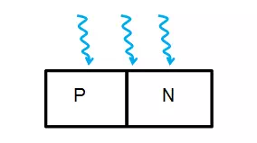
To overcome this problem, we need to apply external energy directly to the depletion region to generate more charge carriers. A special type of diode called photodiode is designed to generate more number of charge carriers in depletion region. In photodiodes, we use light or photons as the external energy to generate charge carriers in depletion region.
Types of photodiodes
The working operation of all types of photodiodes is same. Different types of photodiodes are developed based on specific application. For example, PIN photodiodes are developed to increase the response speed. PIN photodiodes are used where high response speed is needed.
The different types of photodiodes are
- PN junction photodiode
- PIN photodiode
- Avalanche photodiode
Among all the three photodiodes, PN junction and PIN photodiodes are most widely used.
PN junction photodiode
PN junction photodiodes are the first form of photodiodes. They are the most widely used photodiodes before the development of PIN photodiodes. PN junction photodiode is also simply referred as photodiode. Nowadays, PN junction photodiodes are not widely used.
When external light energy is supplied to the p-n junction photodiode, the valence electrons in the depletion region gains energy. If the light energy applied to the photodiode is greater the band-gap of semiconductor material, the valence electrons gain enough energy and break bonding with the parent atom. The valence electron which breaks bonding with the parent atom will become free electron. Free electrons moves freely from one place to another place by carrying the electric current. When the valence electron leave the valence shell an empty space is created in the valence shell at which valence electron left. This empty space in the valence shell is called a hole. Thus, both free electrons and holes are generated as pairs. The mechanism of generating electron-hole pair by using light energy is known as the inner photoelectric effect.
The minority carriers in the depletion region experience force due to the depletion regionelectric field and the external electric field. For example, free electrons in the depletion region experience repulsive and attractive force from the negative and positive ions present at the edge of depletion region at p-side and n-side. As a result, free electrons move towards the n region. When the free electrons reaches n region, they are attracted towards the positive terminals of the battery. In the similar way, holes move in opposite direction.
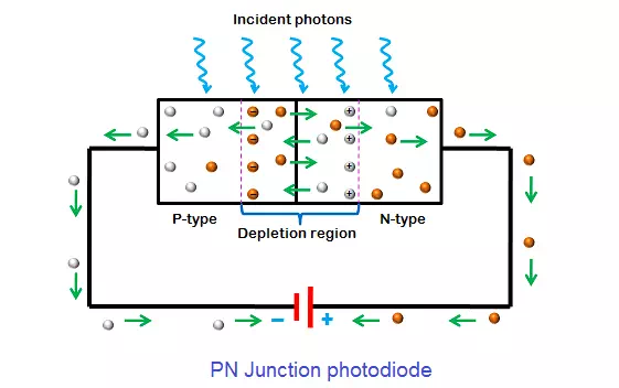
The strong depletion region electric field and the external electric field increase the drift velocity of the free electrons. Because of this high drift velocity, the minority carriers (free electrons and holes) generated in the depletion region will cross the p-n junction before they recombine with atoms. As a result, the minority carrier current increases. When no light is applied to the reverse bias photodiode, it carries a small reverse current due to external voltage. This small electric current under the absence of light is called dark current. It is denoted by I λ. In a photodiode, reverse current is independent of reverse bias voltage. Reverse current is mostly depends on the light intensity.
In photodiodes, most of the electric current is carried by the charge carriers generated in the depletion region because the charge carriers in depletion region has high drift velocity and low recombination rate whereas the charge carriers in n-side or p-side has low drift velocity and high recombination rate. The electric current generated in the photodiode due to the application of light is called photocurrent.
The total current through the photodiode is the sum of the dark current and the photocurrent. The dark current must be reduced to increase the sensitivity of the device. The electric current flowing through a photodiode is directly proportional to the incident number of photons.