Tunnel diode definition
A Tunnel diode is a heavily doped p-n junction diode in which the electric current decreases as the voltage increases. In tunnel diode, electric current is caused by “Tunneling”. The tunnel diode is used as a very fast switching device in computers. It is also used in high-frequency oscillators and amplifiers.
Symbol of tunnel diode
The circuit symbol of tunnel diode is shown in the below figure. In tunnel diode, the p-type semiconductor act as an anode and the n-type semiconductor act as a cathode.
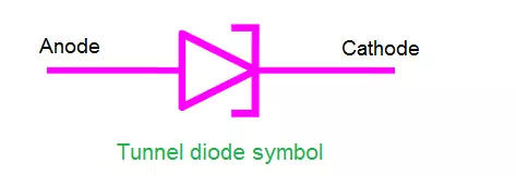
We know that a anode is a positively charged electrode which attracts electrons whereas cathode is a negatively charged electrode which emits electrons. In tunnel diode, n-type semiconductor emits or produces electrons so it is referred to as the cathode. On the other hand, p-type semiconductor attracts electrons emitted from the n-type semiconductor so p-type semiconductor is referred to as the anode.
What is a tunnel diode?
Tunnel diodes are one of the most significant solid-state electronic devices which have made their appearance in the last decade. Tunnel diode was invented in 1958 by Leo Esaki. Leo Esaki observed that if a semiconductor diode is heavily doped with impurities, it will exhibit negative resistance. Negative resistance means the current across the tunnel diode decreases when the voltage increases. In 1973 Leo Esaki received the Nobel Prize in physics for discovering the electron tunneling effect used in these diodes. A tunnel diode is also known as Esaki diode which is named after Leo Esaki for his work on the tunneling effect. The operation of tunnel diode depends on the quantum mechanics principle known as “Tunneling”. In electronics, tunneling means a direct flow of electrons across the small depletion region from n-side conduction band into the p-side valence band.
The germanium material is commonly used to make the tunnel diodes. They are also made from other types of materials such as gallium arsenide, gallium antimonide, and silicon.
Width of the depletion region in tunnel diode
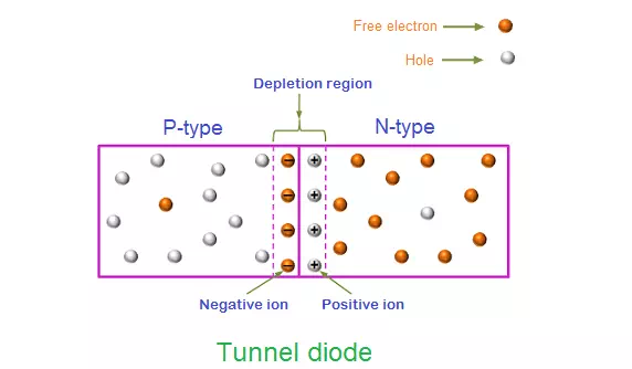
The depletion region is a region in a p-n junction diode where mobile charge carriers (free electrons and holes) are absent. Depletion region acts like a barrier that opposes the flow of electrons from the n-type semiconductor and holes from the p-type semiconductor. The width of a depletion region depends on the number of impurities added. Impurities are the atoms introduced into the p-type and n-type semiconductor to increase electrical conductivity. If a small number of impurities are added to the p-n junction diode (p-type and n-type semiconductor), a wide depletion region is formed. On the other hand, if large number of impurities are added to the p-n junction diode, a narrow depletion region is formed.
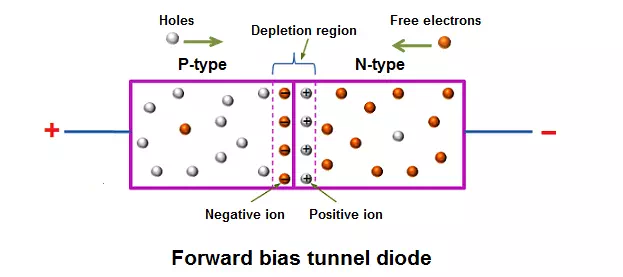
In tunnel diode, the p-type and n-type semiconductor is heavily doped which means a large number of impurities are introduced into the p-type and n-type semiconductor. This heavy doping process produces an extremely narrow depletion region. The concentration of impurities in tunnel diode is 1000 times greater than the normal p-n junction diode. In normal p-n junction diode, the depletion width is large as compared to the tunnel diode. This wide depletion layer or depletion region in normal diode opposes the flow of current. Hence, depletion layer acts as a barrier. To overcome this barrier, we need to apply sufficient voltage. When sufficient voltage is applied, electric current starts flowing through the normal p-n junction diode. Unlike the normal p-n junction diode, the width of a depletion layer in tunnel diode is extremely narrow. So applying a small voltage is enough to produce electric current in tunnel diode. Tunnel diodes are capable of remaining stable for a long duration of time than the ordinary p-n junction diodes. They are also capable of high-speed operations.
Concept of tunneling
The depletion region or depletion layer in a p-n junction diode is made up of positive ions and negative ions. Because of these positive and negative ions, there exists a built-in-potential orelectric field in the depletion region. This electric field in the depletion region exerts electric force in a direction opposite to that of the external electric field (voltage). Another thing we need to remember is that the valence band and conduction band energy levels in the n-type semiconductor are slightly lower than the valence band and conduction band energy levels in the p-type semiconductor. This difference in energy levels is due to the differences in the energy levels of the dopant atoms (donor or acceptor atoms) used to form the n-type and p-type semiconductor.