MOSFET’s make very good electronic switches for controlling loads and in CMOS digital circuits as they operate between their cut-off and saturation regions.
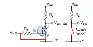
We saw previously, that the N-channel, Enhancement-mode MOSFET (e-MOSFET) operates using a positive input voltage and has an extremely high input resistance (almost infinite) making it possible to interface with nearly any logic gate or driver capable of producing a positive output. We also saw that due to this very high input (Gate) resistance we can safely parallel together many different MOSFETS until we achieve the current handling capacity that we required. While connecting together various MOSFETS in parallel may enable us to switch high currents or high voltage loads, doing so becomes expensive and impractical in both components and circuit board space. To overcome this problem Power Field Effect Transistors or Power FET’s where developed.V We now know that there are two main differences between field effect transistors, depletion-mode only for JFET’s and both enhancement-mode and depletion-mode for MOSFETs. In this tutorial we will look at using the Enhancement-mode MOSFET as a Switchas these transistors require a positive gate voltage to turn “ON” and a zero voltage to turn “OFF” making them easily understood as switches and also easy to interface with logic gates.
The operation of the enhancement-mode MOSFET, or e-MOSFET, can best be described using its I-V characteristics curves shown below. When the input voltage, ( VIN ) to the gate of the transistor is zero, the MOSFET conducts virtually no current and the output voltage ( VOUT ) is equal to the supply voltage VDD. So the MOSFET is “OFF” operating within its “cut-off” region.
MOSFET Characteristics Curves
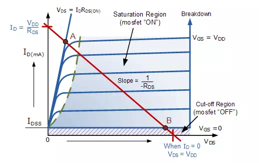
The minimum ON-state gate voltage required to ensure that the MOSFET remains “ON” when carrying the selected drain current can be determined from the V-I transfer curves above. When VIN is HIGH or equal to VDD, the MOSFET Q-point moves to point A along the load line. The drain current ID increases to its maximum value due to a reduction in the channel resistance. ID becomes a constant value independent of VDD, and is dependent only on VGS. Therefore, the transistor behaves like a closed switch but the channel ON-resistance does not reduce fully to zero due to its RDS(on) value, but gets very small. Likewise, when VIN is LOW or reduced to zero, the MOSFET Q-point moves from point A to point B along the load line. The channel resistance is very high so the transistor acts like an open circuit and no current flows through the channel. So if the gate voltage of the MOSFET toggles between two values, HIGH and LOW the MOSFET will behave as a “single-pole single-throw” (SPST) solid state switch and this action is defined as:
Cut-off Region
Here the operating conditions of the transistor are zero input gate voltage ( VIN ), zero drain current ID and output voltage VDS = VDD. Therefore for an enhancement type MOSFET the conductive channel is closed and the device is switched “OFF”.
Cut-off Characteristics
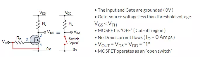
Then we can define the cut-off region or “OFF mode” when using an e-MOSFET as a switch as being, gate voltage, VGS < VTH thus ID = 0. For a P-channel enhancement MOSFET, the Gate potential must be more positive with respect to the Source.
Saturation Region
In the saturation or linear region, the transistor will be biased so that the maximum amount of gate voltage is applied to the device which results in the channel resistance RDS(on being as small as possible with maximum drain current flowing through the MOSFET switch. Therefore for the enhancement type MOSFET the conductive channel is open and the device is switched “ON”.
Saturation Characteristics
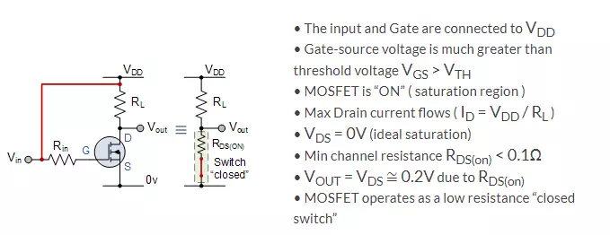
Then we can define the saturation region or “ON mode” when using an e-MOSFET as a switch as gate-source voltage, VGS > VTH thus ID = Maximum. For a P-channel enhancement MOSFET, the Gate potential must be more negative with respect to the Source. By applying a suitable drive voltage to the gate of an FET, the resistance of the drain-source channel, RDS(on) can be varied from an “OFF-resistance” of many hundreds of kΩ, effectively an open circuit, to an “ON-resistance” of less than 1Ω, effectively acting as a short circuit. When using the MOSFET as a switch we can drive the MOSFET to turn “ON” faster or slower, or pass high or low currents. This ability to turn the power MOSFET “ON” and “OFF” allows the device to be used as a very efficient switch with switching speeds much faster than standard bipolar junction transistors.
example of using the MOSFET as a switch
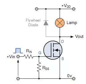
In this circuit arrangement an Enhancement-mode N-channel MOSFET is being used to switch a simple lamp “ON” and “OFF” (could also be an LED). The gate input voltage VGS is taken to an appropriate positive voltage level to turn the device and therefore the lamp load either “ON”, ( VGS = +ve ) or at a zero voltage level that turns the device “OFF”, ( VGS = 0V ). If the resistive load of the lamp was to be replaced by an inductive load such as a coil, solenoid or relay a “flywheel diode” would be required in parallel with the load to protect the MOSFET from any self generated back-emf. Above shows a very simple circuit for switching a resistive load such as a lamp or LED. But when using power MOSFETs to switch either inductive or capacitive loads some form of protection is required to prevent the MOSFET device from becoming damaged. Driving an inductive load has the opposite effect from driving a capacitive load.
For example, a capacitor without an electrical charge is a short circuit, resulting in a high “inrush” of current and when we remove the voltage from an inductive load we have a large reverse voltage build up as the magnetic field collapses, resulting in an induced back-emf in the windings of the inductor. Then we can summarise the switching characteristics of both the N-channel and P-channel type MOSFET within the following table.
| MOSFET Type | VGS (+ve) | VGS (0V) | VGS (-ve) |
| N-channel Enhancement | ON | OFF | OFF |
| N-channel Depletion | ON | ON | OFF |
| P-channel Enhancement | OFF | OFF | ON |
| P-channel Depletion | OFF | ON | ON |
Note that unlike the N-channel MOSFET whose gate terminal must be made more positive (attracting electrons) than the source to allow current to flow through the channel, the conduction through the P-channel MOSFET is due to the flow of holes. That is the gate terminal of a P-channel MOSFET must be made more negative than the source and will only stop conducting (cut-off) until the gate is more positive than the source. So for the enhancement type power MOSFET to operate as an analogue switching device, it needs to be switched between its “Cut-off Region” where: VGS = 0V (or VGS = -ve) and its “Saturation Region” where: VGS(on) = +ve. The power dissipated in the MOSFET ( PD ) depends upon the current flowing through the channel ID at saturation and also the “ON-resistance” of the channel given as RDS(on). For example.