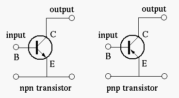
A Bipolar Junction Transistor (BJT) has three terminals connected to three doped semiconductor regions. In an NPN transistor, a thin and lightly doped P-type base is sandwiched between a heavily doped N-type emitter and another N-type collector; while in a PNP transistor, a thin and lightly doped N-type base is sandwiched between a heavily doped P-type emitter and another P-type collector. In the following we will only consider NPN BJTs.
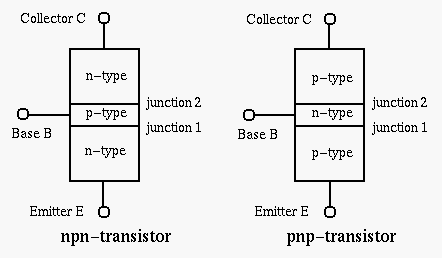
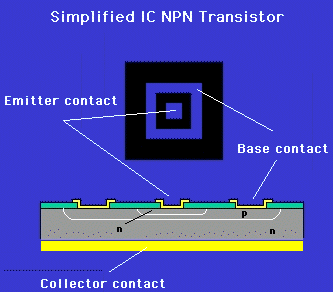
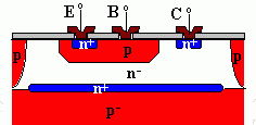
In many schematics of transistor circuits (especially when there exist a large number of transistors in the circuit), the circle in the symbol of a transistor is omitted. The figures below show the cross section of two NPN transistors. Note that although both the collector and emitter of a transistor are made of N-type semiconductor material, they have totally different geometry and therefore can not be interchanged.
All previously considered components (resistor, capacitor, inductor, and diode) have two terminals (leads) and can therefore be characterized by the single relationship between the current going through and the voltage across the two leads. Differently, a transistor is a three-terminal component, which could be considered as a two-port network with an input-port and an output-port, each formed by two of the three terminals, and characterized by the relationships of both input and output currents and voltages. Depending on which of the three terminals is used as common terminal, there can be three possible configurations for the two-port network formed by a transistor:
- Common emitter (CE),
- Common base (CB),
- Common collector (CC).
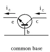
- Common-Base (CB) configuration
Two voltages ![]() and
and ![]() are applied respectively to the emitter
are applied respectively to the emitter ![]() and collector
and collector ![]() , with respect to the common base
, with respect to the common base ![]() , so that the BE junction is forward biased while the CB junction is reverse biased.
, so that the BE junction is forward biased while the CB junction is reverse biased.
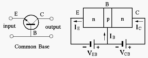
Note that the polarity of ![]() and direction of
and direction of ![]() associated with the PN-junction between E and B are the same as those associated with a diode, voltage polarity: positive on P, negative on N, current direction: from P to N, but
associated with the PN-junction between E and B are the same as those associated with a diode, voltage polarity: positive on P, negative on N, current direction: from P to N, but ![]() and the direction of
and the direction of ![]() associated with the PN-junction between the base and collector are defined oppositely.
associated with the PN-junction between the base and collector are defined oppositely.
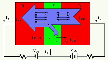
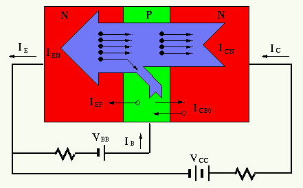
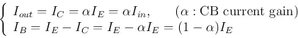
The behavior of the NPN-transistor is determined by its two PN-junctions:
- The forward biased base-emitter (BE) PN-junction allows the free electrons in emitter to go through the PN-junction to arrive at the base, forming the emitter current
 .
. - As the P-type base is thin and lightly doped, only a small number of the electrons from the emitter are combined with the holes in base to form the base current
 .
. - Most of the electrons coming from the emitter become minority carriers in the P-type base, and they go through the reverse biased collector-base PN junction to arrive at the collector.
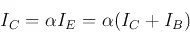
- The percentage of those electrons that arrive at the collector out of the electrons from the emitter is defined as
 (e.g.,
 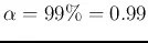 , depending on the doping and geometry of the material). The total collector current
  is therefore
  .
.
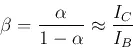
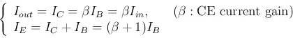
The current gain or current transfer ratio is defined as the ratio between the emitter (input) current ![]() and the collector (output) current
and the collector (output) current ![]() :
:
The base current ![]() is:
is:

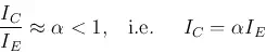
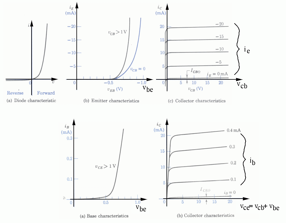
- The CB configuration can be considered as a 2-port circuit. The input port is formed by the emitter and base, the output port is formed by the collector and base. The relationships between the current and voltage of both the input and output ports are described by the following input and output characteristics.
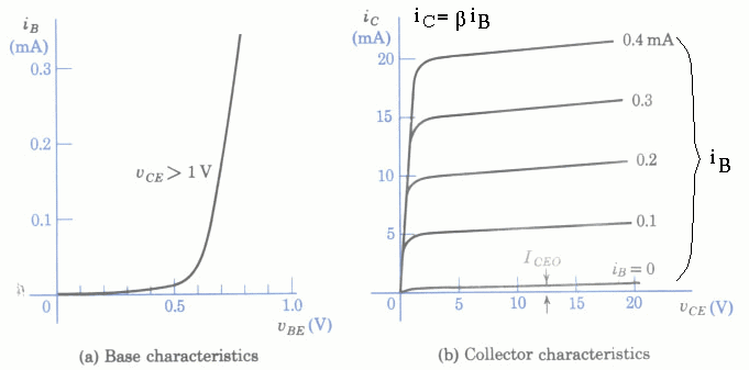
- Input characteristics:
The input current ![]() is a function of
is a function of ![]() as well as the input voltage
as well as the input voltage ![]() , which is much more dominant:
, which is much more dominant:

where
This relationship between ![]() and
and ![]() as the EB junction is very similar to the relationship of
as the EB junction is very similar to the relationship of ![]() and
and ![]() of a diode. Also, we also note higher
of a diode. Also, we also note higher ![]() .
.
- Output characteristics:
The output current ![]() is a function of the output voltage
is a function of the output voltage ![]() as well as the input current
as well as the input current ![]() , which is much more dominant:
, which is much more dominant:
Here the approximation is based on the assumption that ![]() depends totally on
depends totally on ![]() . When
. When ![]() ,
, ![]() is the current caused by the minority carriers crossing the PN-junction. This is similar to the diode current-voltage characteristics seen before, except both axes are reversed (the polarity of
is the current caused by the minority carriers crossing the PN-junction. This is similar to the diode current-voltage characteristics seen before, except both axes are reversed (the polarity of ![]() and the direction
and the direction ![]() are oppositely defined). When
are oppositely defined). When ![]() is increased,
is increased, ![]() is increased correspondingly. Higher
is increased correspondingly. Higher ![]() can slightly increase
can slightly increase ![]() . As
. As ![]() , CB configuration does not have current-amplification effect. However, if
, CB configuration does not have current-amplification effect. However, if ![]() is held constant,
is held constant, ![]() and therefore
and therefore ![]() will also be held constant, i.e., CB transistor circuit can be used as a current source.
will also be held constant, i.e., CB transistor circuit can be used as a current source.
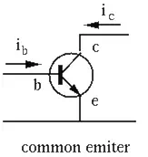
- Common-Emitter (CE) configuration
Two voltages ![]() and
and ![]() are applied respectively to the base
are applied respectively to the base ![]() and collector
and collector ![]() with respect to the common emitter
with respect to the common emitter ![]() . As typically
. As typically ![]()

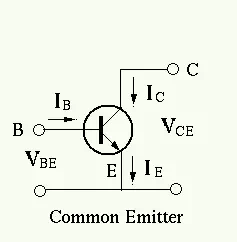
The base current ![]() is treated as the input current, and the collector current
is treated as the input current, and the collector current ![]() is treated as the output current:
is treated as the output current:
Solving this equation for ![]() , we get the relationship between the output
, we get the relationship between the output ![]() and the input
and the input ![]() :
:
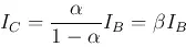
where we have defined the CE current gain, the ratio of the output current ![]() and the input current
and the input current ![]() :
:
The two parameters ![]() and
and ![]() are related by any of the following:
are related by any of the following:

For example, if ![]() , then
, then ![]() .
.
The CE configuration can be considered as a 2-port circuit. The input port is formed by the base and emitter, the output port is formed by the collector and emitter. The relationships between the current and voltage of both the input and output ports are described by the following input and output characteristics.
- Input characteristics:
Same as in the case of common-base configuration, the EB junction of the common-emitter configuration can also be considered as a forward biased diode, the current-voltage characteristics is similar to that of a diode:

![]() has little effect on
has little effect on ![]() .
.
- Output characteristics:

Higher ![]() .
.
The CB junction is reverse biased, the current ![]() depends on the current
depends on the current ![]() . When
. When ![]() ,
, ![]() , the current caused by the minority carriers crossing the PN-junctions. When
, the current caused by the minority carriers crossing the PN-junctions. When ![]() is increased,
is increased, ![]() is correspondingly increased by
is correspondingly increased by ![]() fold.
fold.
The relationship between the input and output currents of both CB and CE configurations is summarized below:
- CB
- CE
The collector characteristics of the common-base (CB) and common-emitter (CE) configurations have the following differences:
- In CB circuit is slightly less than , while in CE circuit
 is much greater than .
 - In CB circuit,
 ; while in CE circuit
  when
when  (as
(as  has the effect of suppressing ).
 - Increased
 will slightly increase but more greatly increase
  , thereby causing more significantly increased .
 - in CB is a function of two variables
 and
and  , but the former is much more significant then the latter. in CE is a function of two variables and , but the former is much more significant then the latter.
 - in CB is a function of two variables and . When is small, its slight increase will cause significant increase of . But its further increase will not cause much change in due to saturation (all available charge carriers travel at the saturation velocity to arrive at collector C), is mostly determined by .
- in CE is a function of two variables and . When is small (
 ), its slight increase will cause significant increase of . But when
  due to saturation (all available charge carriers travel at the saturation velocity to arrive at collector C), is mostly determined by .
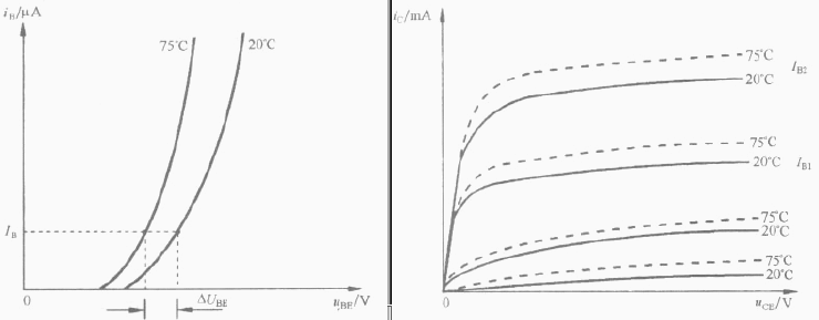
Various parameters of a transistor change as functions of temperature. For example, ![]() increases along with temperature.
increases along with temperature.
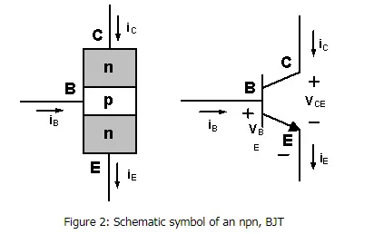
Bipolar Junction Transistor (BJT) is a Semiconductor device constructed with three doped Semiconductor Regions (Base, Collector and Emitter) separated by two p-n Junctions, Figure 1. The p-n Junction between the Base and the Emitter has a Barrier Voltage (V0) of about 0.6 V, which is an important parameter of a BJT. Unlike the Field Effect Transistor (FET), in which Current is produced only by one type of Charge Carrier (Electrons or Holes), in BJT, Current is produced by both types of Charge Carriers (Electrons and Holes), hence the name Bipolar.
Bipolar Junction Transistor
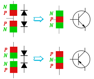
There are two Types of BJT: npn and pnp. The npn Type consists of two n-Regions separated by a p-Region. The pnp Type consists of two p-Regions separated by an n-Region. Figures 2 and Figure 3 are their schematic symbols respectively. The following explanation focuses on the npn BJT.

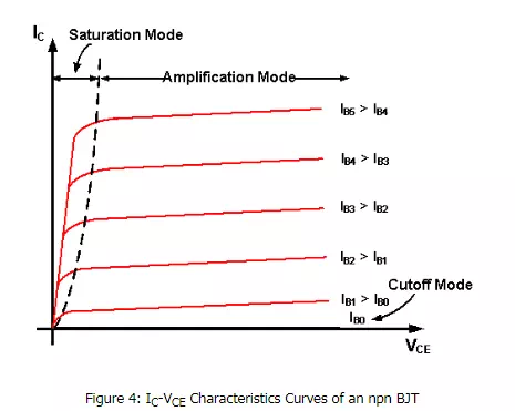
The BJT operates in three different modes: Cutoff mode, Linear Amplification mode and Saturation mode, Figure 4. Table 1 is a summary of the three Operation Modes of an npn BJT.
BJT is very important in electronics. They are used extensively in other Exhibits, especially as Amplifiers in analog circuit and Electronic Switches in digital circuit.