Electronic devices are inherently sensitive to very high frequencies. Most shunt capacitive effects that can be ignored at lower frequencies because the reactance XC = 1/2πfC is very large (open-circuit equivalent). This, however, cannot be ignored at very high frequencies. XC will become sufficiently small due to the high value of f to introduce a low-reactance “shorting” path. In the p-n semiconductor diode, there are two capacitive effects to be considered. Both types of capacitance are present in the forward- and reverse-bias regions, but one so outweighs the other in each region that we consider the effects of only one in each region.
In the reverse-bias region we have the transition- or depletion-region capacitance (CT), while in the forward-bias region we have the diffusion (CD) or storage capacitance.
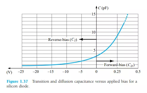
Recall that the basic equation for the capacitance of a parallel-plate capacitor is defined by C = ϵA/d, where ϵ is the permittivity of the dielectric (insulator) between the plates of area A separated by a distance d. In the reverse-bias region there is a depletion region (free of carriers) that behaves essentially like an insulator between the layers of opposite charge. Since the depletion width (d) will increase with increased reverse-bias potential, the resulting transition capacitance will decrease, as shown in Fig. 1.37. The fact that the capacitance is dependent on the applied reverse-bias potential has application in a number of electronic systems.
Although the effect described above will also be present in the forward-bias region, it is overshadowed by a capacitance effect directly dependent on the rate at which charge is injected into the regions just outside the depletion region. The result is that increased levels of current will result in increased levels of diffusion capacitance. However, increased levels of current result in reduced levels of associated resistance (to be demonstrated shortly), and the resulting time constant (τ = RC), which is very important in high-speed applications, does not become excessive.
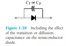
The capacitive effects described above are represented by a capacitor in parallel with the ideal diode, as shown in Fig. 1.38. For low- or mid-frequency applications (except in the power area), however, the capacitor is normally not included in the diode symbol.
